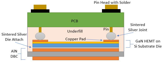
Fig.1. Side view of the simplified active region of the PCB-Interposer-on-DBC structure
Gallium nitride (GaN) high electron mobility transistors (HEMTs) show great promise for high-frequency and high-temperature switching operations in power converters. However, to fully utilize their advantages, their packages must be designed to minimize the junc-tion-to-case thermal resistance and parasitic electrical parameters. To achieve minimal package parasitic inductances, an example of previous efforts involved embedding bare transistor dice into printed circuit boards (PCBs). However, this packaging approach suffers from large junc-tion-to-case thermal resistance because of PCB materials low thermal conductivity. It also suf-fers from low thermomechanical reliability because of the large coefficient of thermal expansion mismatch between the GaN device and PCB. To improve the thermal performance and reliability of the embedded packaging, CPES recently developed a PCB-Interposer-on-Direct Bonded Copper (DBC) packaging approach and applied it to packaging GaN Systems 650 V, 120 A GaN HEMT die. As shown in Fig. 1, the die is sandwiched between an aluminum nitride (AlN) DBC substrate and a PCB. The DBC substrate provides electrical isolation and heat extraction, while gold-plated pins through the PCB connect the die terminals to the PCB circuit for low parasitic inductances.
To investigate the thermo-mechanical reliability of the PCB-Interposer-on-DBC package, a finite-element analysis tool, ANSYS Mechanical, is used to simulate the temperature-cycling test of the package and find the stress and strain distributions at the packages intercon-nects. Shown in Fig. 2 is a FEA model of half of the package undergoing a temperature cycling test between -40 to 125 °C. One focus of the analysis is on the sintered silver joints con-necting the PCB to the device. Results of the simulations include the shear and normal stresses at the joints, and the volume averaged strain energy density per thermal loading cycle (VA SED/cycle). The latter is a widely accepted metric for evaluating the reliability or predicting the lifetime of a bonded interconnect.
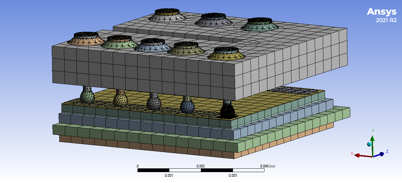
Fig. 2. Half model being simulated with the underfill re-moved for clarity


