


LIBRARY
Passive Balancing of Peak Currents between Paralleled MOSFETs with Unequal Threshold Voltages
Year: 2017 | Author: Yincan Mao | Paper: D3.9
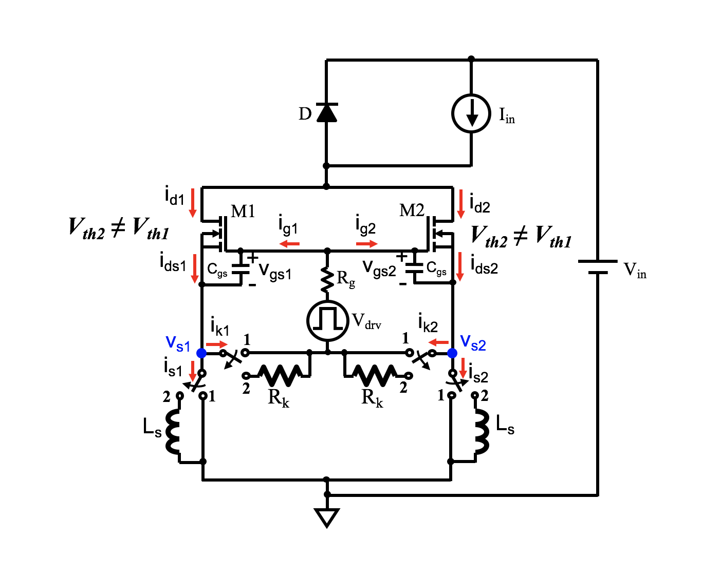
Fig. 1. Influence of power-source inductance (Ls) and drive-loop resistance connected to the source (Rk) on dynamic sharing, where the lower side is paralleled SiC MOSFETs with mismatched Vth and upper side is a SiC Schottky barrier diode.
The influence of power-source inductance (Ls) and drive-loop resistance connected to the source (Rk) on dynamic sharing with mismatched threshold voltage and balanced layout is shown in Fig. 1. The scheme with two switches for every branch represents different structures (with symmetry maintained); the influences of Ls and Rk on dynamic sharing can be tested. The para-sitics of the package are not included in the analysis for simplicity. However, the theory holds up well when parasitics are considered, as shown in the experimental verification (Fig. 2), which in-cludes parasitics from the device package and copper traces. The DPT (double-pulse tester) is used for the testing of switching transients.
Fig. 2 shows the experimental results with designed Ls and Rk. The desired current sharing is obtained within one switching cycle by utilizing a single gate driver. Better sharing is also achieved for the turn-off transient as compared to the baseline, shown in Fig 2(a).
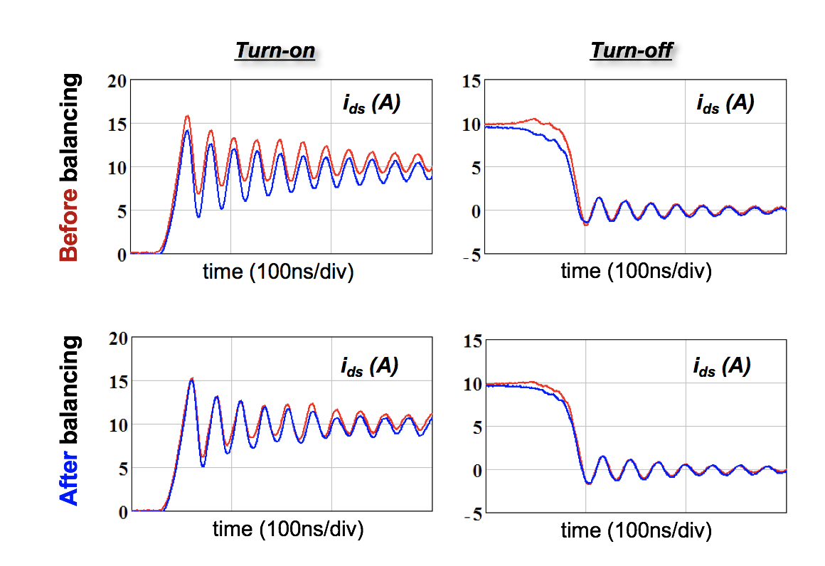
Fig. 2. Experimental results tested at Vin = 300 V, Iin = 20 A, Rg + 0.5Rk = 20 &Omega, Vth1 = 2.34 V, Vth2 = 2.78 V for verification of current balancing solu-tion in Fig. 1. Drain-source currents for turn-on and turn-off transients (a) Without Ls and R design, and (b) With Ls and Rk design.
