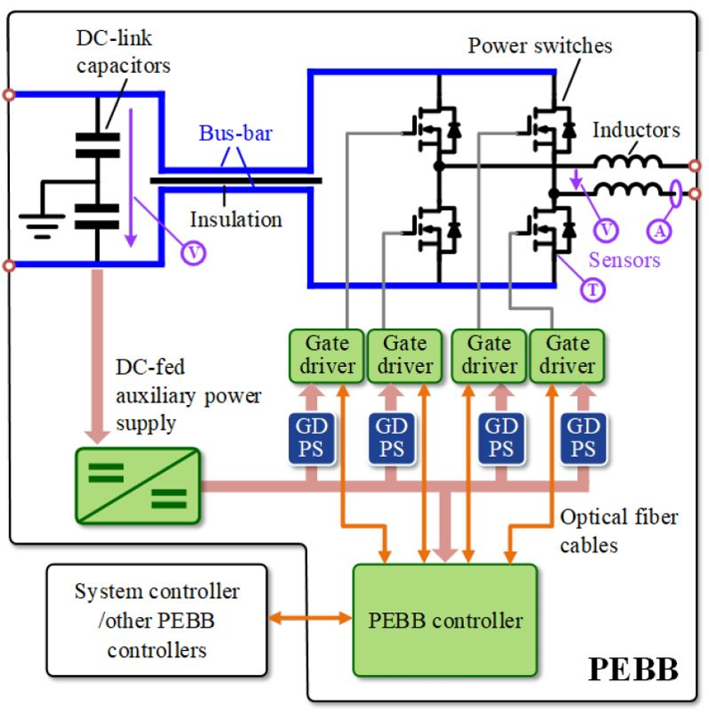
Fig.1. PEBB6000 system architecture diagram.
A power electronics building block (PEBB) has been defined as a universal power processor, featuring modular configurations, scalable voltage, and current ratings, as well as low inventory and maintenance cost. In the past two decades, nearly all of the commercial high-power converters took advantage of the PEBB concept in medium voltage (MV) and high-voltage (HV) applications. Those PEBBs are connected in series, parallel, or multiple-phase configurations to scale up the voltage and current ratings of PEBB-based converters, breaking through the constraints of the semiconductor device ratings. In recent years, as a result of the booming technology of wide bandgap semiconductor devices and packaging, silicon carbide (SiC) MOSFETs have demonstrated their superior performance to silicon (Si) insulated-gate bipolar transistors (IGBTs) in terms of higher breakdown voltage, faster switching speed, lower switching loss, and higher operating temperature. The high blocking voltage of SiC MOSFETs simplifies the PEBB power stage, (shown in Fig. 1), by using uncomplicated topologies. Their high switching frequency preserves the overall harmonic performance, despite a reduced number of voltage levels. The design and testing of smart gate drivers, gate driver power supplies, and the laminated DC bus-bar were explored, and all of them showed excellent performance. The H-bridge power stage and gate drivers were integrated into a plastic enclosure, shown in Fig. 2, a test platform for further assessment. The remaining parts of the PEBB6000 design will be published in the future. The gate driver is the critical interface between the power semiconductor devices and control signals. It serves to provide galvanic isolation and to supply driving current, while maintaining signal integrity under a high-noise environment. In addition to those basic tasks, it provides quick, reliable, and configurable protection, as well as advanced switch-current signal sensing and data processing for control purposes, which define a smart gate driver. The gate driver power supply must withstand the voltage stress between its primary and secondary sides, as well as having a low input-output parasitic capacitance to reduce the CM noise current. In this design, a resonant converter that offers a resonant current bus (RCB) to drive multiple isolated load is proposed, and achieves 20 kV isolation and only 1.56 pF of input-to-output parasitic capacitance. For the laminated busbar design, three different possibilities are evaluated. The option with the midpoint on top of the positive and negative busbar performed the best in terms of losses and fringing flux.
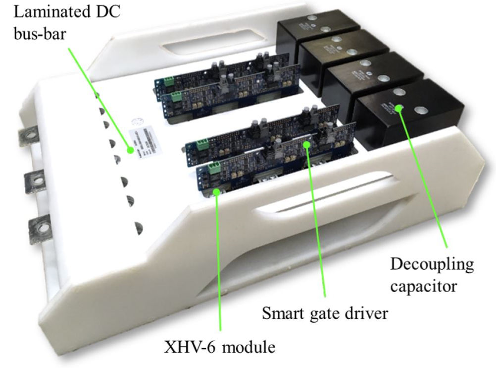
Fig. 2. PEBB6000 prototype integrating XHV-6 mod-ules, gate drivers, and the laminated DC bus-bar.


