


LIBRARY
Evaluation of an Automated Modeling Tool Applied to New 600 V, 2 A Vertical GaN Transistors
Year: 2020 | Author: Grace Watt | Paper: T1.21
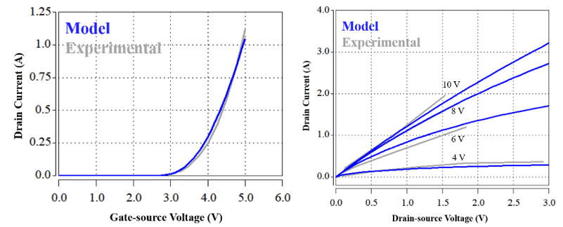
Fig. 1. Vertical GaN transfer and output characteristics comparison measured with a drain-source voltage of 10 V at 25° C.
This paper demonstrates effective models of wide bandgap devices that accurately simulate switching time and parasitic ringing. The primary investigation compares the experimental and modeled static and dynamic behavior of HRLs 600 V, 2 A vertical GaN transis- tor. The properties of GaN devices, and more specifically, vertically oriented GaN devices, could allow for efficient performance at high frequency and high power. The experimental turn-on and turn-off times are 8.48 ns and 30.2 ns, demonstrating the potential for high frequency applications with GaN. Firstly, a SiC example indicated that SaberTM is effective at creating an accurate subcircuit model when given output, transfer, and on-state resistance curves obtained experimentally or from a datasheet. The SiC static data matched with a maximum error of 11.3%, and the dynamic behavior demonstrated minimal error as the model in a test circuit would produce accurate timing and loss. The GaN model had a maximum error of 8.42% for output, transfer, and Rds(on) characteristics. It switched within a couple nanoseconds of the experimental times, and the parasitic ringing accurately represented the rise and fall times so that the modeled loss and timing would be accurate in test simulation. A critical method- ological finding for model development was the accuracy of parasitic ringing frequency and magnitude afforded by optimizing the para- sitic elements in the model circuits. Furthermore, the rates of rise and fall matched more closely with this technique.
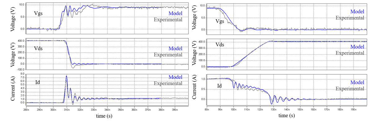
Fig. 2. SaberTM GaN turn-on and turn-off waveforms with optimized parasitic circuit elements at a drain-source voltage of 400 V, a 1 A load current, and 2.5 ? gate resistance at 25° C.
