


LIBRARY
Investigation of Pyroelectric Polarization Effect On GaN MOS Capacitors and Field-Effect Transistors
Year: 2013
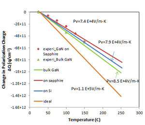
Fig. 1. Polarization charges vs. Temperature for
GaN capacitors on different substrates.
GaN capacitors on different substrates.
We prepared both GaN MOS capacitors and MOSC-HEMTs on different substrates. One of the capacitor samples was fabricated on a commercial (0001) UID GaN epitaxial layer grown by MOCVD on sapphire substrate, while the other was on a bulk GaN substrate. PECVD SiO22. Then 500nm of Al was used to form contacts. The three MOSC-HEMTs have the same device structure except for its epi. They were fabricated on 30nm UID Al0.22Ga0.78N on 3µm UID GaN on sapphire substrate (MOSC-HEMT 1), 20nm UID GaN cap on 20nm UID Al0.25Ga0.75N on GaN buffer on Si (111) substrate (MOSC-HEMT 2), and 22nm UID Al0.23Ga0.77N on UID GaN on bulk GaN (MOSC-HEMT 3). ICP etch was used to remove the AlGaN layer as well as the 2DEG in the channel in order to get enhancement-mode devices. Wet etch was done right afterwards to remove surface damages. 100nm PECVD SiO2 was deposited on MOSC-HEMT 1 and 3, while 50nm on MOSC-HEMT 2, followed by 30 min annealing at 1000°C in N2. Ti/Al was deposited and annealed at 400°C for 15min for n ohmic contacts. We measured the Capacitance-Voltage characteristics of the two capacitors from 23°C to 150°C, and the I-V for the MOSC-HEMTs from 23°C to 250°C. The flatband voltage shifts positively with increasing temperature, which gives us a pyroelectric voltage coefficient of 7.4104 V/m-K and 8.5104 V/m-K for sapphire and bulk GaN substrate. We fit the experimental plots with the piezoelectric constants given by F. Bernardini [3] and the lattice parameters in Table I, as shown in Fig. 1. Since the calculated ideal bulk GaN (without lattice mismatch) curve does not fit the experimental value, we estimate the lattice mismatch to be 50%. The threshold voltage shift for MOSC-HEMT in Fig. 2 seems more complex than the capacitors since we are measuring the current across the channel, instead of directly measuring the induced charge. We attribute the differences to the change of interface traps and mobile charges with increasing temperature.
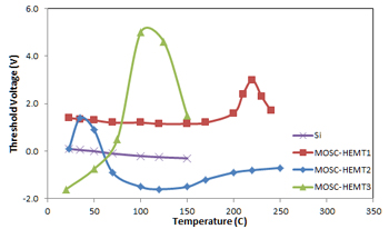
Fig. 2. Threshold voltage shift vs. Temperature for GaN MOSC-HEMTs on different substrates.
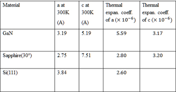
Fig. 3. Lattice parameters and thermal expansion coefficients for calculation.
