


LIBRARY
EMI Evaluation of a 1.7 kV SiC MOSFET Module with Organic DBC Substrate
Year: 2021 | Author: Narayan Rajagopal | Paper: S13.6
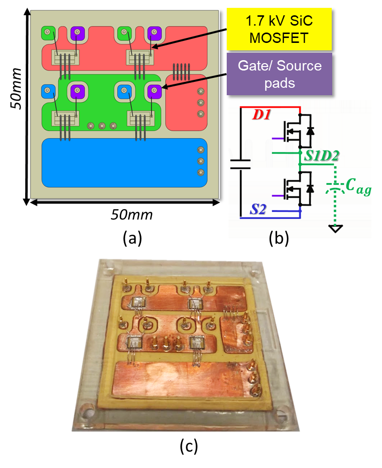
Fig.1. (a) ODBC-based half-bridge layout, (b) Half-bridge schematic, and (c) ODBC module prototype.
A 1.7 kV SiC MOSFET half-bridge module was fabricated using a 50 mm × 50 mm ODBC substrate as shown in Fig. 1(c) . The layout of the module is shown in Fig. 1(a). The Cu pads are colorcoded to correspond to the nodes in the schematic shown in Fig. 1(b). The half-bridge was designed to minimize CM noise by reducing the S1D2 area to be less than 30 % of the total substrate area. The ODBC module was simulated in a custom inverter testbed, where the input and output impedance of the system are equal (Zin = Zout). This allows for a simplified common-mode equivalent model (CEM) of the testbed.
The ratio of the S1D2 capacitance (Cag) to the total module capacitance to ground (Cbp ) can be manipulated to minimize or cancel the leakage current through the baseplate. The testbed and model were previously verified with a Cree BM2 SiC MOSFET power module. As shown in Fig 2, the baseplate leakage current of the ODBC module is reduced by nearly 20 dB across a wide frequency range, and by 30 dB at 5-10 MHz. This evaluation is valuable because it demonstrates that proper application of a suitable CM model can be employed to reduce emissions in a deterministic fashion, even without the introduction of CM filters.

Fig. 2: Predicted leakage current through module baseplate in (a) time-domain, (b) frequency-domain for practical configuration of EMI testbed with commercial module (red) and ODBC module (blue)
This work was supported by the Office of Naval Research (ONR) with the grant number N00014-16-1-2956
