


LIBRARY
Evaluation of Low-Pressure-Sintered Multi-Layer Substrates for Medium-Voltage SiC Power Modules
Year: 2021 | Author: Jacob Gersh | Paper: S5.5
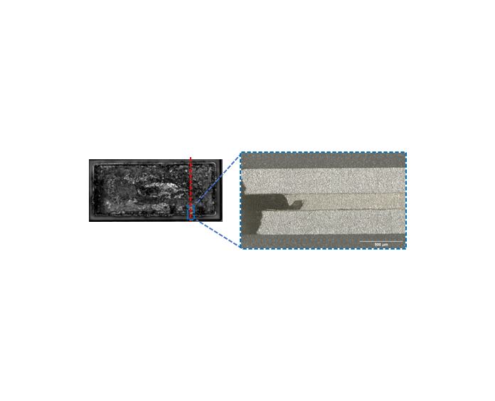
Fig. 1: C-SAM images of (a) nano-silver paste sample before (left) and after (right) 300 thermal cycles from 40 °C to 200°C, and (b) a nano- silver preform sample before (left) and after (right) 300 cycles. Cross-sections are cut and imaged at the dotted red lines after 300 thermal cycles.
The reliability of the multi-layer structure was evaluated through thermal cycling tests from -40 °C to 200 °C. Fifteen substrate stacks were fabricated for reliability testing. Four samples were bonded with nano-silver paste using 1 MPa pressure, and 11 samples were fabricated with nano- silver preform and either 1 MPa or 3 MPa pressure. The nano-silver preform sintering time is 90 seconds, while the nano-silver paste must be sintered for 1 hour. The samples fabricated with the nano-silver preform and 3 MPa sintering pressure were the most uniform of the population, according to the C-SAM images. Fig. 1 shows the location of cross-sections taken on samples after 300 thermal cycles. The C-SAM image Fig. 1(a) suggests voids in the silver bond line for the nano-silver paste sample. The nano-silver preform sample imaged in Fig. 1(b) showed more uniformity, and no abnormalities are present in the C-SAM image after 300 thermal cycles. The samples shown in Fig. 1 were cross-sectioned, polished, and imaged with a digital microscope. No obvious failure in the bond layer of either sample is shown in either cross-section. However, small cracks are observed at the edges of the bond of the nano-silver paste sample (Fig. 1(a)). Cross-sections of additional nano-silver paste and preform samples will be imaged after 300, 400, and 500 thermal cycles to better identify the onset and propagation of voids and cracks.
