


LIBRARY
Characterization of 4.5 kV Charge-Balanced SiC MOSFETs
Year: 2021 | Author: Jack Knoll | Paper: S13.2
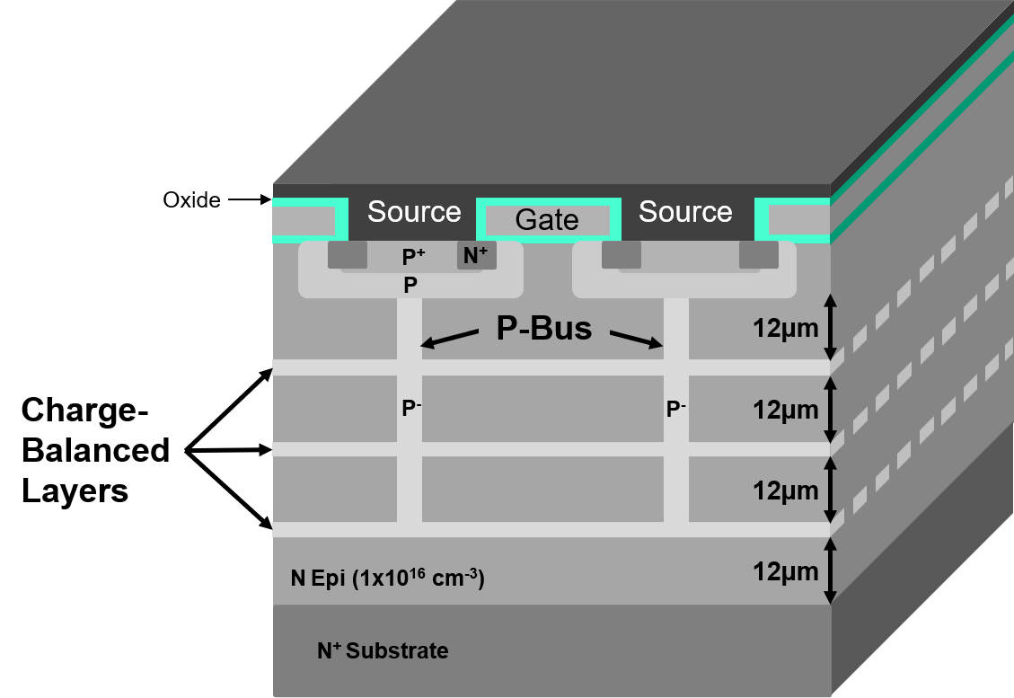
Fig. 1. 4.5 kV SiC CB MOSFET.
A Keysight B1505A curve tracer was used to characterize the CB SiC MOSFETs. The devices with the wide and large pitch bus design (WL) have the lowest on-resistance, while the devices with the wide and small pitch bus design (WS) have the highest on-resistance. Distinct steps in the output and Miller capacitance-voltage curves are caused by a rapid increase in depletion width as the individual depletion boundaries surrounding a single JFET or CB region meet.
A double-pulse inductive switching test (DPT) was used to evaluate the dynamic performance of the CB SiC MOSFETs up to 3 kV. These devices experience a turn-on voltage tail at room temperature caused by the slow transition to conduction of the depleted N-epi layer. The turn-on voltage tail of the devices was found to be dependent on temperature (Fig. 2), blocking voltage, drain current, and p-bus structure. The turn-on tail is lowest for the type WS devices because they have the highest amount of p-doped bus per unit volume. Operating the SiC CB MOSFETs at higher temperatures reduces the voltage fall time by nearly four times. Above 100° C, the voltage tail becomes essentially negligible.
A 4.5 kV silicon IGBT (IXYX40N450HV) was evaluated using the same DPT setup. At 150° C, the total turn-on energy of the type WS CB SiC MOSFET is more than twelve times lower than that of the silicon IGBT. SiC CB MOSFETs hence offer advantages over silicon IGBTs in higher frequency applications due to their superior switching performance at common operating junction temperatures. The low switching loss at high temperatures, superior relationship between specific on-resistance and breakdown voltage, and simplified fabrication processes of SiC CB MOSFETs makes them uniquely qualified for medium-voltage applications.
Acknowledgement: The information, data, or work presented herein was funded in part by the Advanced Research Projects Agency-Energy (ARPA-E), U.S. Department of Energy, under Award Number DEAR0000674 advised by Program Director Isik Kizilyalli. The views and opinions of authors expressed herein do not necessarily state or reflect those of the United States Government or any agency thereof.
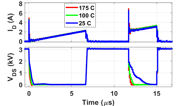
Fig. 2. Switching waveforms at 25° C, 100° C, and 175° C for device type WS.
