


LIBRARY
Improved Measurement Accuracy for Junction-to-Case Thermal Resistance of GaN HEMT Packages by Gate-to-Gate Electrical Resistance and Stacking Thermal Interface Materials
Year: 2022 | Author: Shengchang Lu | Paper: T-S1.1
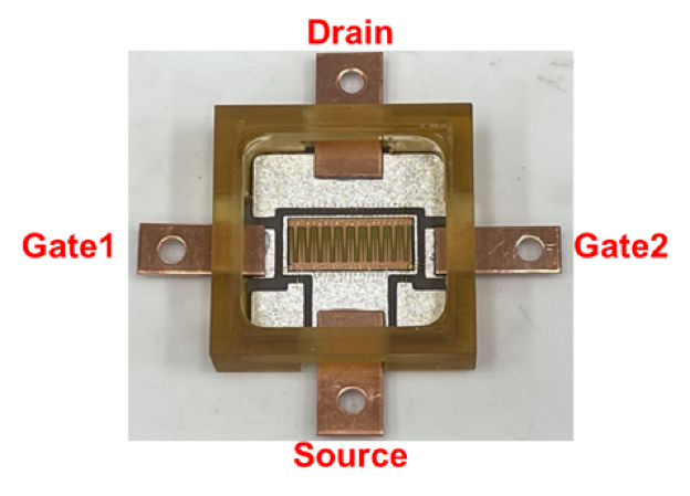
Fig. 1. Top view of a completed eGaN package.
However, the common TSEPs of a GaN HEMT lack sufficient sensitivity or stability due to charge trapping effect from device switching action. Recently, researchers fabricated GaN HEMT devices with two gate pads. They showed that the gate end-to-end or gate-to-gate electrical re-sistance, Rg2g, can be used as a reliable TSEP. However, because they did not fabricate pack-ages for their devices, they did not apply the technique to measure RthJC.
In this work, we packaged a commercial (650 V, 150 A) eGaN device with two gate pads for the purpose of accurately measuring RthJC of the GaN package in Fig. 1. Two techniques were combined to improve the accuracy: (1) using Rg2g as the TSEP and (2) making multiple thermal re-sistance measurements with stacked layers of a thermal interface material (TIM). The stacked-TIM technique was employed to reduce inaccuracy in determining the package case temperature. The measurement procedure was tested using two different types of TIM on a custom package of an eGaN (650 V, 150 A) HEMT. In Fig. 2, the two measured RthJC were found within 24% of each other.
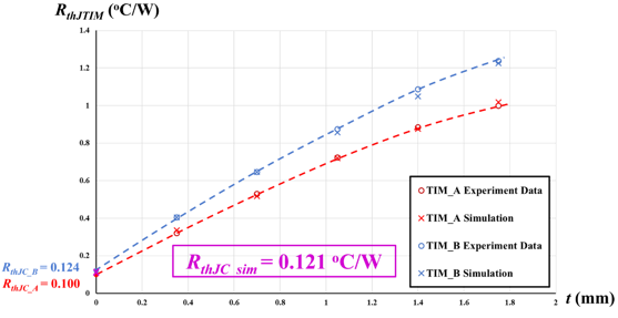
Fig. 2. Plots of the measured (red and blue circles) and simulated (red and blue crosses) junction-to-TIM thermal resistances with each TIM type. The dash lines are the fitted curves. The intercepts of the fitting curves on the y-axis are the experimentally determined RthJC.
