


LIBRARY
PCB Winding Coupled Inductor Design and Common-Mode EMI Noise Reduction for Soft-Switching Three-Phase AC-DC Converter
Year: 2022 | Author: Gibong Son | Paper: T-S2.2

Fig. 1. Circuit topology for two-channel interleaved three-phase ac-dc converter with balance technique.
A balance technique can effectively lessen the CM noise. In Fig.1, the two-channel interleaved three-phase ac-dc converter with the balance technique is presented. The circuit topology requires the additional return path connecting from the middle point of the dc capacitors, m, to the neutral point of the ac filter capacitors, n. In the return path, additional inductors are placed to form a balance structure. The inductors on the return path are coupled with the inductors in the main circuit for better balance at high frequency.
The converter is implemented with PCB winding magnetics. The PCB winding coupled inductor needs to be carefully designed by taking into account a variety of considerations: 1) Winding configuration to minimize the winding loss, 2) placement of the return path to maximize the cou-pling between the main inductors and the additional inductors, 3) coupling coefficient between main inductors to reduce switching frequency range, device loss, and core loss, 4) turns number of the main inductors to balance out the winding loss and the core loss. By properly design the PCB winding inductor, CM Noise can be effectively reduce up to almost 15 MHz as shown in Fig. 2.
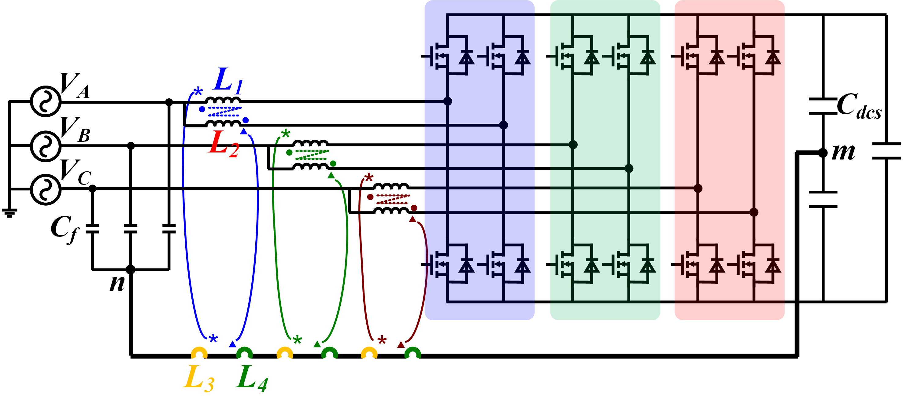
Fig. 2.Comparison of measured CM EMI Noise between litz-wire inductor without balance technique and PCB winding coupled inductor with balance technique
