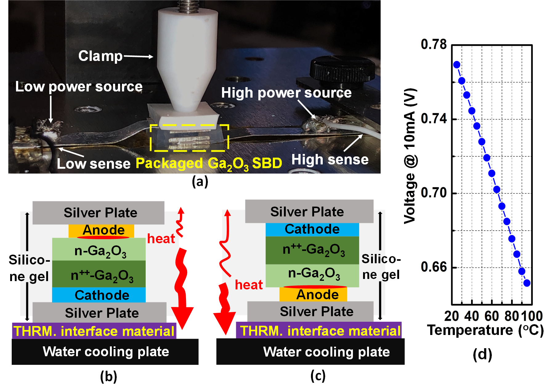
Fig. 1. (a) Photo of the test setup. Schematic of Rθ measurements under (b) bottom-side cooling and (c) junction-side cooling. (d) The forward voltage at 10 mA current as a function of temperature of the pack-aged Ga2O3 SBD.
The low thermal conductivity of Ga
2O
3 has arguably been the most serious concern for Ga
2O
3 power and RF devices. Despite many simulation studies, there is no experimental report on the thermal resistance of a large-area, packaged Ga
2O
3 device. This work fills this gap by demonstrating a 15-A double-side packaged Ga
2O
3 Schottky barrier diode (SBD) and measuring its junction-to-case thermal resistance (
RθJC) in the bottom-side- and junction-side-cooling configurations. The
RθJC characterization is based on the transient dual interface method, i.e., JEDEC 51-14 standard, and the test set-up is shown in Fig. 1. Fig. 2 shows the
RθJC of the junction- and bottom-cooled Ga
2O
3 SBD was measured to be 0.5 K/W and 1.43 K/W, respectively, with the former
RθJC lower than that of similarly-rated commercial SiC SBDs. This low
RθJC is attributable to the heat extraction directly from the Schottky junction instead of through the Ga
2O
3 chip. The
RθJC lower than that of commercial SiC devices proves the viability of Ga
2O
3 devices for high-power applications and manifest the significance of proper packaging for their thermal management.
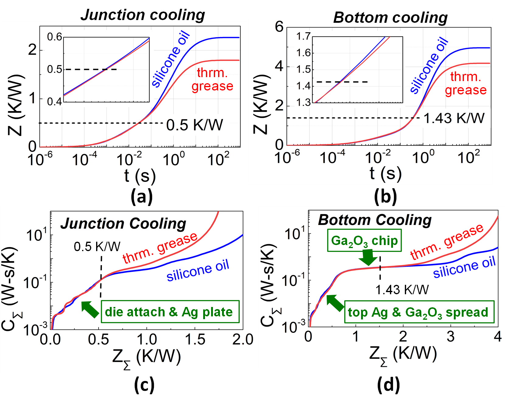
Fig. 2. Transient thermal impedance curves of the Ga2O3 SBD measured with two TIMs under the (a) junction- and (b) bottom-side cooling. The insets show the zoom-in plot of the separation point. Calcu-lated structure function with two TIMs in the (c) junction- and (d) bottom-side cooling.


