


LIBRARY
Design, Fabrication, and Testing of a 1.7 kV SiC Switching Cell for a High-Density Integrated Power Electronics Building Block (iPEBB)
Year: 2022 | Author: Narayan Rajagopal | Paper: T-S1.5
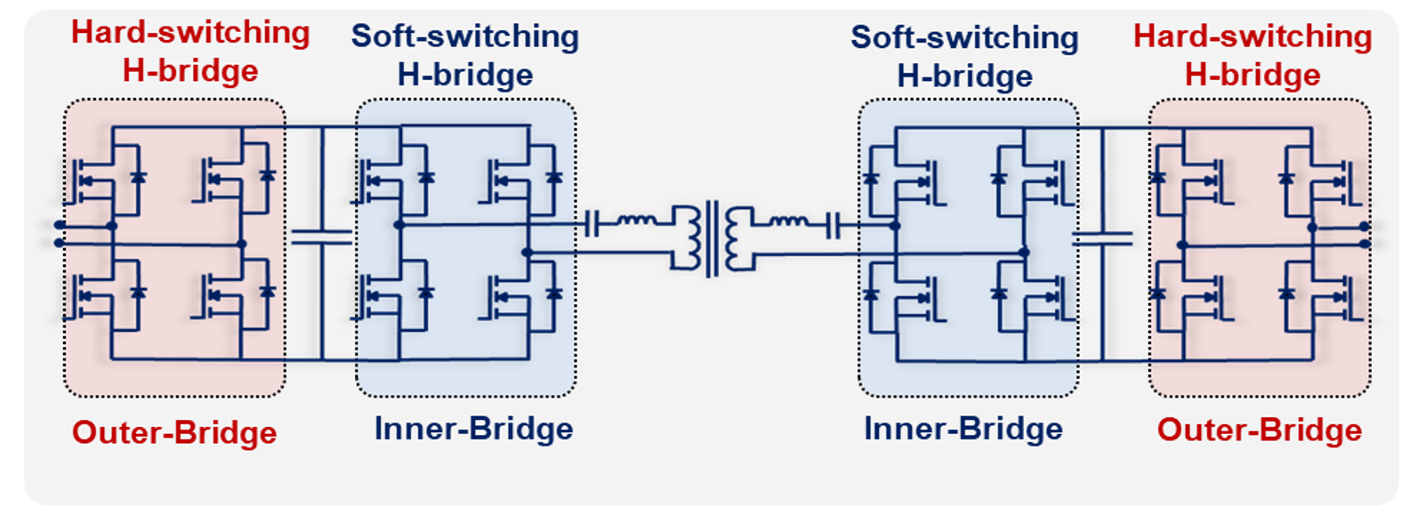
Fig 1. Bi-directional topology for iPEBB with hard- and soft-switching H-bridges
Fig. 2 shows the fabricated iPEBB switching cell. It is populated with two parallel 1.7 kV SiC MOSFETs per switch. State-of-the-art multi-layer silicon nitride active metal brazed (AMB) substrates are used to develop a low inductance design for the iPEBB. The multi-layer design is made up of three copper layers divided by two silicon nitride dielectric layers. Vias connect the top copper layer to a middle copper layer which enables a vertical power loop and negative mutual inductance cancellation. This cancellation allows for a reduced power-loop inductance of 3.5 nH. Furthermore, the multi-layer design creates an inherent screen that reduces the common-mode current through the cooling system. The multi-layer design uses thick copper layers which enable good heat spreading. The copper layers of the switching cell were optimized to improve thermal performance while minimizing the weight increase of the iPEBB.
Initial electrical testing was completed on the switching cell to see its dynamic performance. Double pulse tests at 1 kV and 50 A were completed. The voltage fall time during turn-on is 20 ns and has a turn-on dv/dt of 40 V/ns with an overshoot of approximately 9%. The voltage rise time during turn-off is 10.3 ns and gives a dv/dt of 77 V/ns. Furthermore, the switching cell was designed to maximize the heat-spreading capabilities while minimizing the weight of the iPEBB. The measured junction-to-case thermal resistance of the switching cell is 0.285° C/W, which is comparable to single-layer ceramic substrates. The switching-cell design, fabrication, and testing will go into advancing -based PEBBs for future power systems.
This work was supported by the Office of Naval Research (ONR), with grant number N00014-16-1-2956.
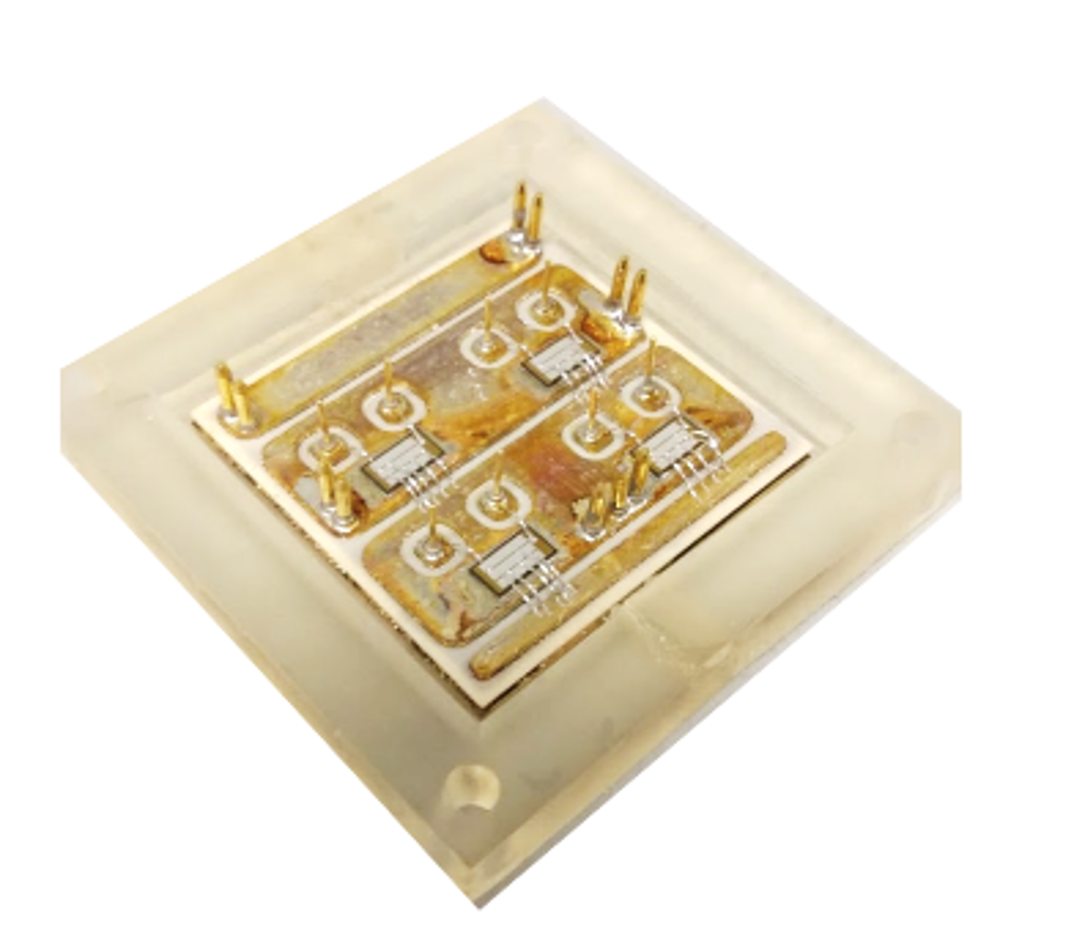
Fig 2. Prototype of fabricated switching cell
