LIBRARY
High-Frequency PCB-Winding Transformer Design with Medium Voltage Insulation for Solid-State Transformer
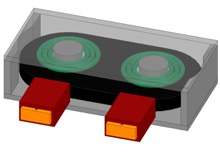
In this paper, a compact printed circuit board (PCB) -winding transformer structure is proposed to handle medium-voltage insulation by FR4 in the PCB winding. The primary-side winding is built into the PCB winding and the secondary-side winding is still Litz wire to allow for lower loss. Such an insulation structure lifts the partial-discharge inception voltage with an even thinner FR4 thickness. With semi-conductive shielding and the stress grading layer design, the E-field can be restrained in the primary-side PCB, which enables partial-discharge-free insulation. An arc section winding structure is proposed to reduce the high E-field inside the insulation layer to improve insulation performance.
The electric performance and the transformer optimization process are also discussed in detail. The transformer loss is optimized considering the high winding loss on the primary-side PCB winding with the layer-to-layer winding resistance. The overall size and loss trade-off is analyzed to provide a low-loss design as well as better thermal management.
Finally, the transformer prototype is built and the design is demonstrated on an 800/400V, 15kW, 200kHz CLLC converter. The peak efficiency reaches 98.8% and the power density is 130W/in3. The transformer also passes the insulation test, whereby the partial-discharge-free level is up to 14.6 kV.


