


LIBRARY
Electro-Thermal Device-Package Co-Design for Ultra-Wide Bandgap Gallium Oxide Power Devices
Year: 2023 | Author: Benjamin Lyon | Paper: H1.12
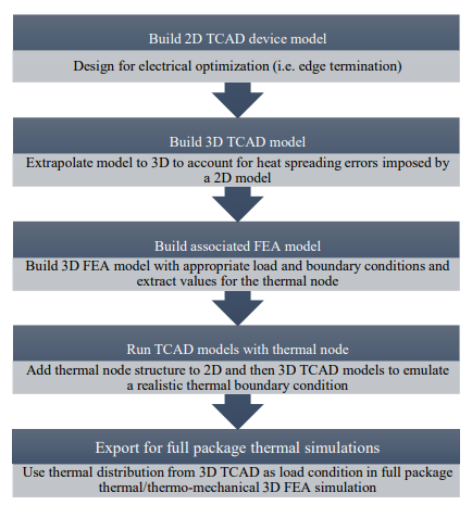
Fig.1. Proposed co-design process flow.
In this work, several modeling methods are explored for an electrothermal device package co-design. The first method selected was a 3D finite element analysis (FEA) multiphysics simulation, which is widely used due to its low computational demands and ability to model not only the heat interactions between material interfaces but also a convection coefficient at the boundary. However, the micro-/nano-scale device structures, lattice-based heating, and thermally dependent electrical parameters are not all modeled. The 2D and 3D physics-based technology computer-aided design (TCAD) models account for these physics effects, but the high computational power required due to the large difference in length scales between the electrically active regions (e.g., nanometer-sized edge termination structures and drift regions) and the thermal diffusion regions (e.g., millimeter-sized packaging structures) as well as the involved physics-based solution method limits their use when package components need to be considered. In addition, TCAD does not have the ability to model a convection coefficient; instead it is limited to conductive heat transfer. These approaches were compared, and it was ascertained that a combination of FEA and TCAD models, detailed in Fig. 1., was warranted for an accurate and efficient electrothermal co-design.
This allows for analysis of the relationship between device structures and the resulting junction temperature and thermal distribution. As a test case, the device thickness, area, and anode diameter were varied to evaluate their impact on thermal performance. TABLE I summarizes the effectiveness of the different device structure modifications that were explored. They are compared to the baseline case, which has a junction temperature of 344°C.
This work outlines and evaluates an electro-thermal device/package co-design model. This process can be utilized for the efficient and accurate modeling of Ga2O3 devices including any hot spots caused by self-heating that would guide the package requirements and design, as well as the impacts of this heating on the electrical performance.
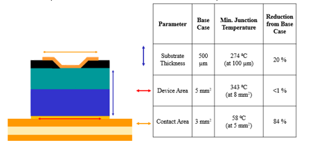
TABLE I. Impact of Ga2O3 device dimensions on thermal perfor-mance.
