LIBRARY
Insulation Design for a Compact, Medium Voltage Transformer
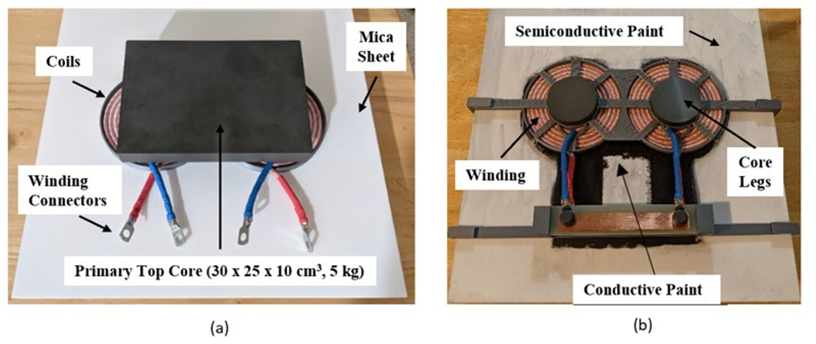
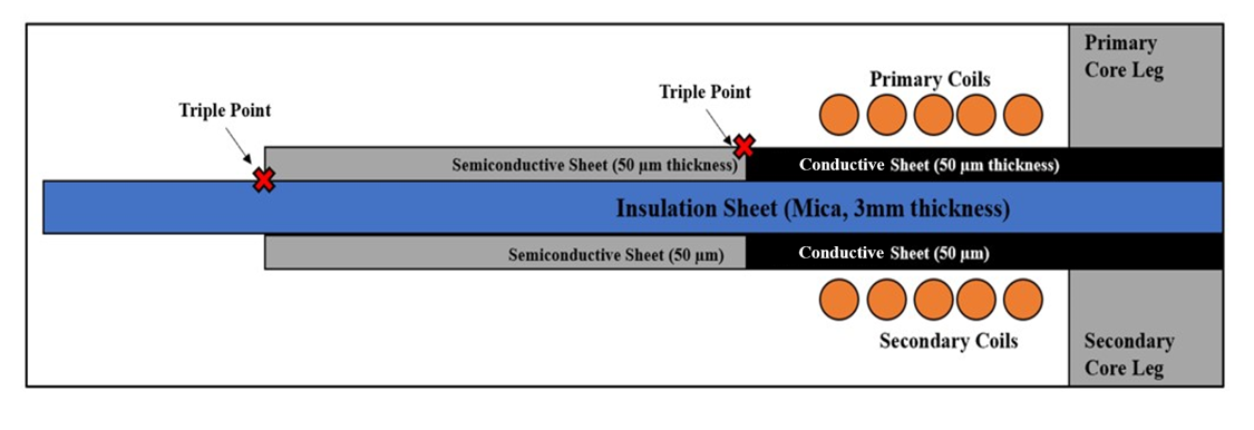
2D electric field simulations were conducted in Ansys Maxwell to understand the location and magnitudes of the critical electric fields for the proposed insulation design. Initial electric field simulations resulted in a peak electric field of 24.4 MV/m and 16.8 MV/m for DC and AC solvers, respectively. The conductivity of the semiconductive sheet was then swept to find the ideal value for electric field reduction and the triple points. A conductivity of 63.1 μ S/m resulted in an 82% reduction in the peak electric field to 2.9 MV/m. Another option for reducing the peak electric field is to replace this linear semiconductive material with a nonlinear resistive coating. The impact of a copper grounding frame was also explored, resulting in over 90% reduction in the critical electric field, to 0.09 MV/m. Two high-potential (HiPot) tests were performed: one with the semiconductive paint, and one with a NLRC. The NLRC was introduced as the simulation indicated that the semiconductive paint is not sufficient to reduce the critical electric fields. By using an NLRC paint instead, the transformer was able to successfully pass the HiPot test at 30 kVAC for > 1 min, which is a typical test criterion for 13.8 kVAC equipment. The proposed transformer prototype is 7.5 K and 5 kg, achieves 99.5% efficiency, and passed a 30 kVAC HiPot test. This work demonstrates a new insulation design that can be used for high-power, MV applications where high-power density and light weight are key.


