LIBRARY
Noise Propagation Study on Gate Drivers Caused by Near Field Coupling inside Medium Voltage High Power SiC-based Converters
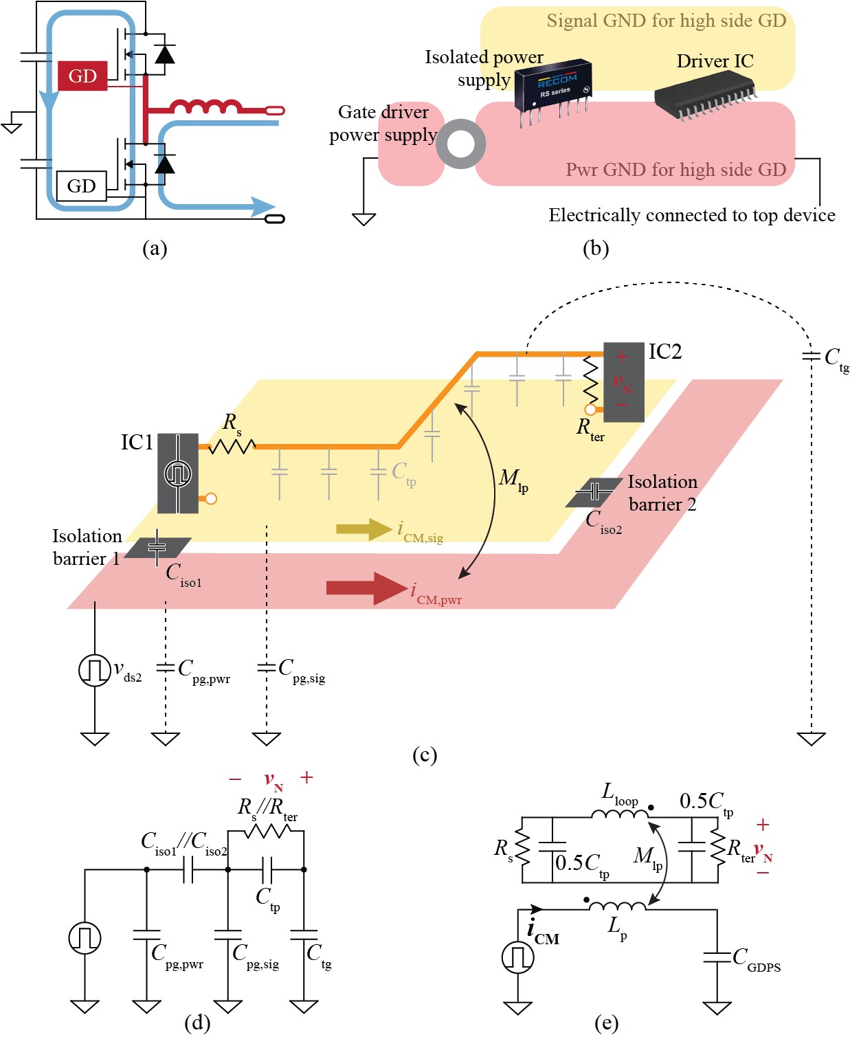
This paper proposes a generic methodology for studying the mechanisms by which noise is induced and propagated on low-power logic circuitry, caused by the switching transient of the high-power main circuit power stage, and hence how it causes the malfunction of important circuits. The noise at the input pins of the critical integrated circuits (ICs) is the point of interest. It is found out that the near fields (both magnetic and electrical) are crucial to the noise propagation. For the magnetic near field, the mutual inductance between the critical signal loop and any di/dt objects will induce voltage noise at the input pins of that IC, leading to potential false triggering. For the electric near field, the printed circuit board (PCB) that is connected to the high-dv/dt node is the major concern; specifically, the parasitic capacitances between the trace, PCB ground, and the converter's local ground will determine how much voltage will be induced on the trace. Proposed noise propagation models are built, and the noises caused by both near fields are theoretically derived and numerically verified by experiments. Factors that influence the noise coupling are also investigated. The factors related to the magnetic near field include the common-mode (CM) current distribution path, as well as the location, length, orientation, shape, and routing layer of the critical signal traces; those related to the electric near field include the distance between the jumping PCB and the converter ground, as well as the source and terminating impedance of the trace.


