


LIBRARY
A Simple and Accurate Method to Characterize Output Capacitance Losses of GaN HEMTs
Year: 2023 | Author: Qihao Song | Paper: T2.2
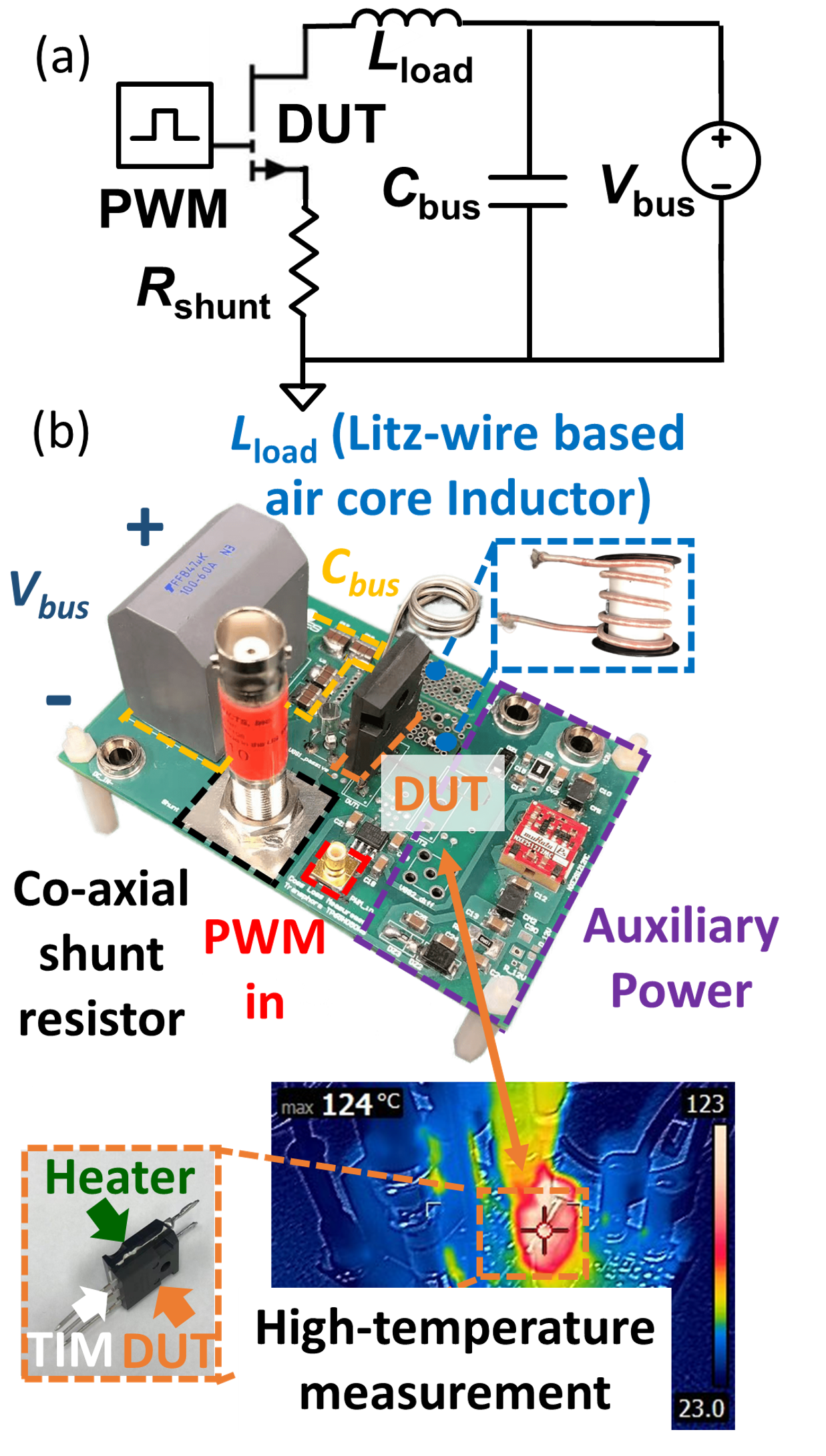
Fig.1. (a) Schematic of the UIS circuit, and (b) phtoto of the exemplary test system for TO-247 packaged devices at 125 ?.
This work proposes a new, easy-to-implement, accurate approach for characterizing the EDISS in a single pulse and under steady-state switching with various operation conditions. The proposed new EDISS characterization method is based upon the unclamped inductive switching (UIS) circuit, as shown in Fig. 1. It consists of a power supply (Vbus) in series with a load inductor (Lload) and the device under test (DUT). A UIS test mainly contains three stages: in stage I, the DUT is ON, Lload is charged by Vbus; in stage II, the DUT is OFF, Lload resonates with the DUT's COSS for about a half resonance cycle, which mimics the device operation in resonant converters; in stage III, the DUT conducts reversely, and the resonance gradually attenuates (see Fig. 2(a)). Vbus is selected as 5 V. Fig. 1(b) shows a photo of the prototyped test system. The DUT's COSS loss can then be derived by subtracting other losses from the total loss in stage II. With careful design and optimization, the DUT's EDISS dominates the total loss, as shown in Fig. 2(b). This ensures a high degree of measurement accuracy.
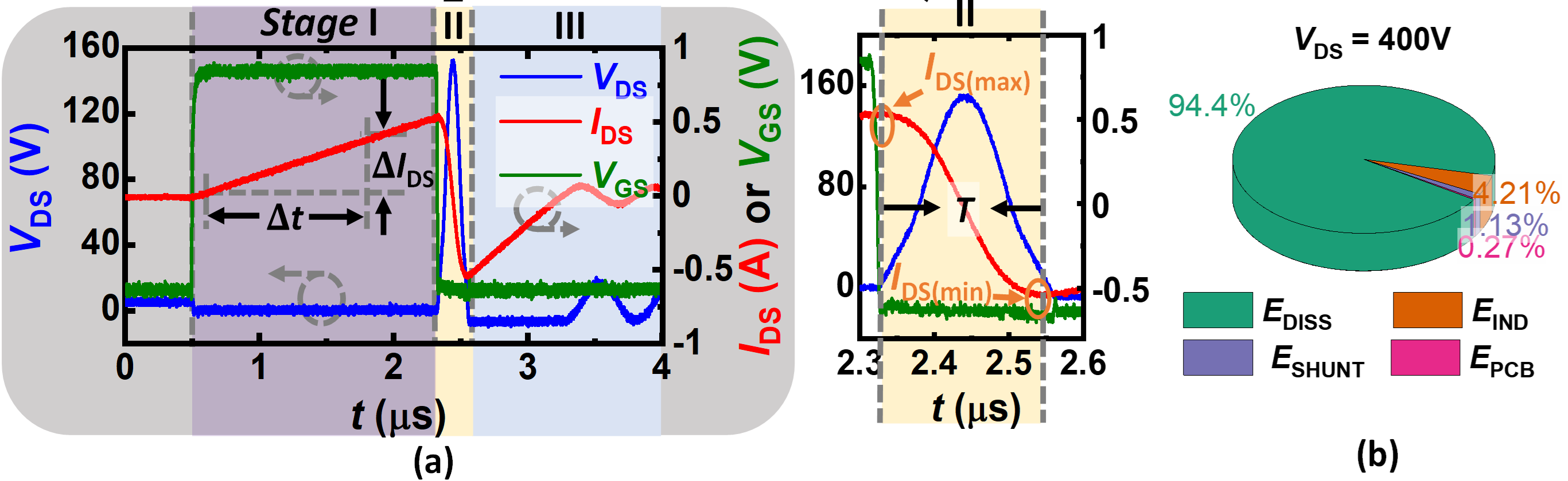
Fig.2. A typical UIS waveform for the extraction of EDISS, and (b) loss breakdown in the UIS.
Building on this new measurement approach, the COSS losses of commercial GaN HEMTs with various designs and from different vendors have been systematically characterized. The impacts of several parameters (including dv/dt, switching frequency, ON-state current, OFF-state voltage, and temperature) on the COSS loss of various GaN HEMTs are revealed. These results provide direct information for GaN device selection and loss evaluation in high-frequency, soft-switching converters.
