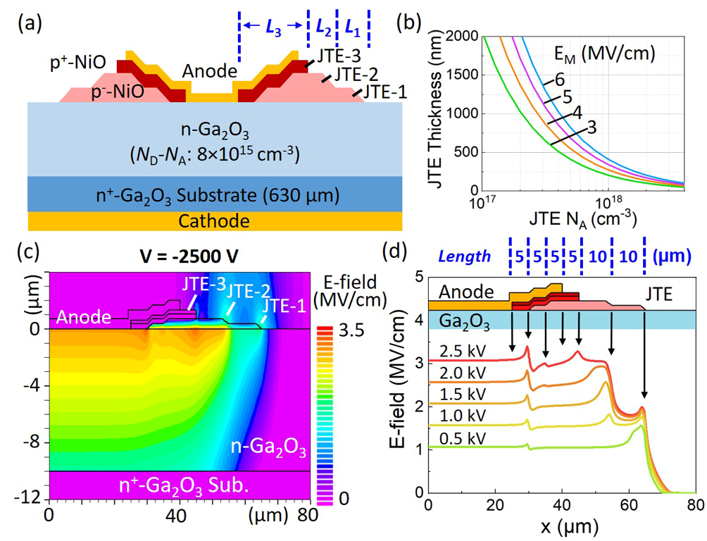
Fig. 1. (a) Schematic of the Ga2O3 SBD with NiO JTE. (b) Simulated E-field contour at 2500 V. (d) E-field profile in Ga2O3 at voltages from 0.5 to 2.5 kV.
Gallium oxide (Ga
2O
3) has emerged as a promising material for future power devices, due to its ultra-wide bandgap, high critical electric field, controllable doping, and large-diameter wafer availability. In various Ga
2O
3 devices, vertical Ga
2O
3 Schottky barrier diodes (SBDs) are advancing fast towards applications. This work demonstrates vertical Ga
2O
3 Schottky barrier diodes (SBDs) with a novel junction termination extension (JTE) comprising multiple layers of sputtered p-type nickel oxide (NiO). The NiO layers have varied lengths to enable a graded decrease in effective charge density away from the main junction. Fig. 1 shows the device schematic and the simulated electric field contours, revealing that the JTE can effectively spread the electric field at the device edge.
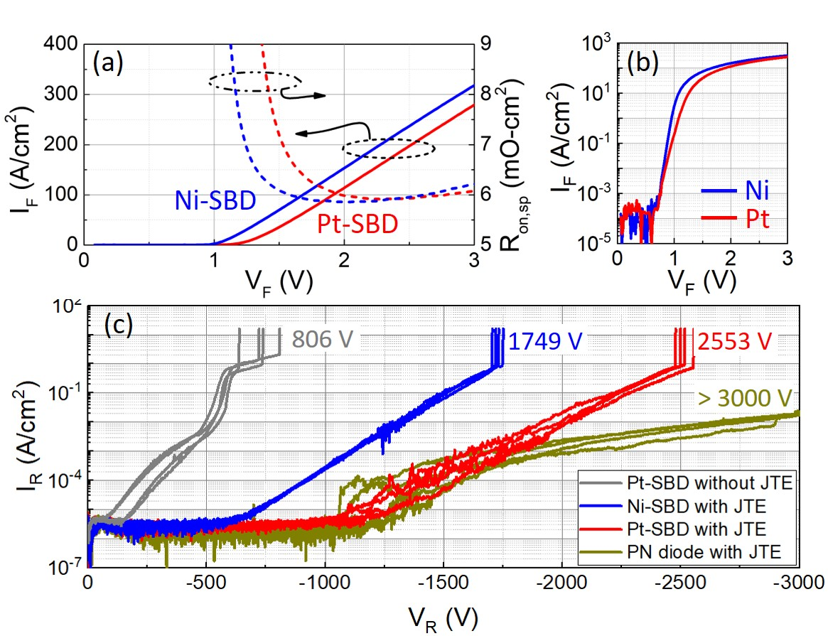
The fabrication of this JTE obviates the etch or implantation and shows good throughput. Two Schottky metals without different work functions (Ni and Pt) are used in device fabrication. The use of Pt is found to be critical to lowering the leakage current and exploiting the JTE functionality. As shown in Fig. 2, the fabricated Ga
2O
3 SBDs exhibit a forward voltage below 1.9 V at the current density of 100 A/cm
3, a differential specific on-resistance of 5.9 mΩ.cm
2, and a breakdown voltage over 2.5 kV.

Fig. 2. Forward I-V characteristics in (a) linear and (b) semi-log scale. (c) Reverse I-V characteristics of non-JTE SBDs, Pt-SBDs, Ni-SBDs, and PN-diodes (PNDs). Four devices at different sample locations are shown for each device type.
The Baliga's figure of merit (FOM) exceeds 1 GW/cm
2 and is among the highest in multi-kilovolt Ga
2O
3 SBDs. Besides, the capacitance of the JTE region is extracted, allowing for evaluation of the capacitance, charge, and switching FOM of 1.7 kV-class Ga
2O
3 SBDs with varied current ratings. The results show good promise of Ga
2O
3 SBDs for kilovolt power electronics.
