


LIBRARY
Avalanche Capability in GaN Vertical PN Diode with Simple Edge Termination
Year: 2023 | Author: Yifan Wang | Paper: H1.4
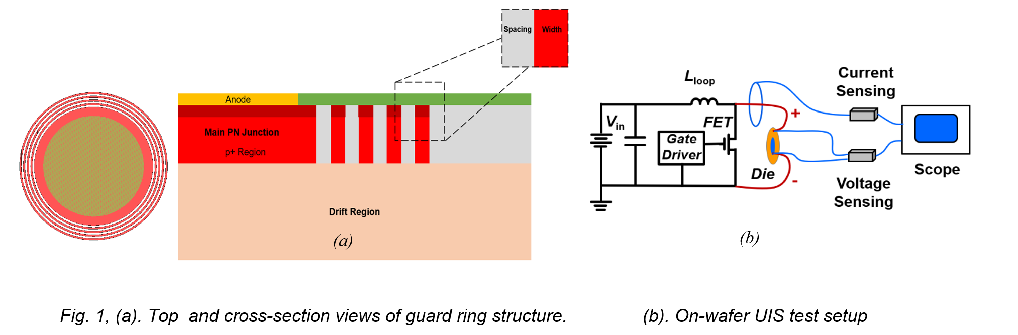
Fig. 1. (a). Top and cross-section views of guard ring structure, and (b). On-wafer UIS test setup
In this work, GaN diodes with floating guard rings that can effectively manage the electric field at the edge are first investigated by technology computer-aided design (TCAD) simulation. The guard ring number, spacing, and implantation depth have been optimized. Fig. 1(a) shows the top and cross-section views of a GaN device with four guard rings. The gray area shown in Fig. 1(a) is created by implanting deep donor-level defects (nitrogen vacancy) into the p+ region.
After the device fabrication, static characterizations are first conducted. A positive temperature coefficient of breakdown voltage has been demonstrated, which is strong evidence for the avalanche capability of guard ring devices. An on-wafer UIS test is then conducted to validate the avalanche robustness under switching conditions. Fig. 1(b) shows the on-wafer UIS test setup. Multiple devices are tested, with some guard ring designs enabling the strong avalanche capability. Fig. 2 shows a guard ring device with voltage-clamping and resistive-energy dissipation, proving the avalanche capability
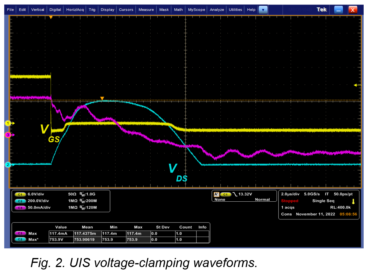
Fig. 2. UIS voltage-clamping waveforms.
This work demonstrates a simple and effective edge termination to enable the avalanche in GaN devices; this approach shows good promise for expanding GaN's applicability in power electronics.
