


LIBRARY
Design of CLLC Converter with High Power and Wide Gain Range
Year: 2023 | Author: Chunyang Zhao | Paper: T1.5
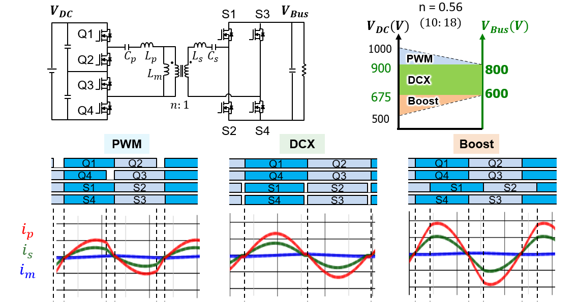
Fig. 1. Circuit topology and waveforms of three-mode operations.
However, in high-power wide-gain-range applications, there is hardly a solution that meets both constraints.
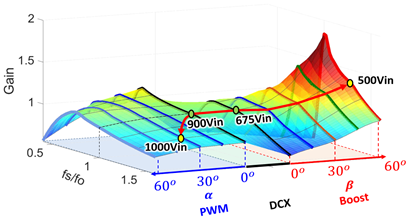
Fig. 2. 3D gain curves and operating path.
Thus, several control methods are combined to solve the problem. In general, the converter will operate in DCX mode when the input voltage is in the nominal voltage range to maximize the peak efficiency, and will operate in boost mode when the input voltage is lower than nominal values to boost gain, and will operate in pulse-width modulation (PWM) mode when the input voltage is higher than nominal values to reduce switching frequency and device losses.
