LIBRARY
Effects of Trace Layout and Encapsulation on Breakdown Voltage in PCB

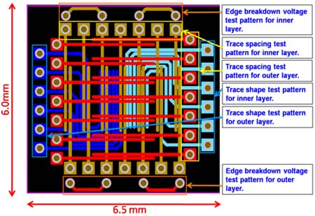
A PCB trace test pattern is designed to test the impacts of the trace clearance, edge clearance, and the winding shape on the breakdown voltage of the PCB traces, as illustrated in Fig. 1. The trace clearances to be tested are 178 µm (7 mil), 255 µm (10 mil), 305 µm (12 mil), 381 µm (15 mil), 508 µm (20 mil). The edge clearances to be tested are 255 µm (10 mil), and 381 µm (15 mil). The winding shape to be tested is 45 degree angle with the trace clearance varied as previous. The PCB board tested is one 4 layer PCB manufactured from Sierra Proto Express.
The test of breakdown voltage for PCB are measured with a Hipotronics H300B Series HiPot at room temperature, i.e. 27°C. The voltage applied between traces is increased to breakdown voltage or 6 kV, which is the maximum DC voltage could be applied on from this device. From the test results, the surface traces pairs on surface layer would breakdown at about 4 kV. In order to increase the breakdown voltage, the outer layer traces are covered with Nusil. The new test results show that if Nusil are properly applied over PCB traces, all surface trace breakdown voltage would be improved to more than 6 kV.


