.jpg)
Fig. 1. (a) Low-profile inductor substrate based on 2-layer PCB: Conceptual drawing.
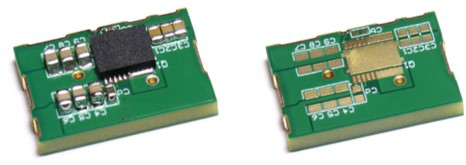
The large thickness of the conventional discrete magnetic component is often the bottleneck for the media and high current POL converter achieving high power density. The low-profile LTCC inductor can work as the substrate of the 3D integrated POL module to improve power density. However, the ceramic-based integration is not cost effective, because high-temperature sintering and complicated assembling processes are involved. This work justifies the feasibility of using SENFOLIAGE (SF) alloy flake composite for the high-frequency PCB integrated POL module. SENFOLIAGE is a composition of alloy flake and epoxy developed by NEC-Tokin. Compared with the traditional flake composite, the permeability and core loss of SENFOLIAGE are improved prominently by doing some lateral alignment of the flake and increasing the volume ratio of the alloy. The compatibility of the flake material with conventional PCB manufacturing technique has been studied, and the layer-wise magnetic core is sandwiched into the multi-layer PCB using the PCB laminating technique, after which the key properties of the SF flake core are kept almost the same.The winding of the inductor is built by the copper layers and conventional PCB vias. Fig. 1 illustrates the conceptual drawing and a prototype of a two-turn low-profile PCB embedded inductor substrate.
As a demonstration of system integration, a 20A, MHz integrated POL module is designed and fabricated based on a 4-layer PCB substrate with an embedded inductor, which achieves more than 85% efficiency and 600W/in
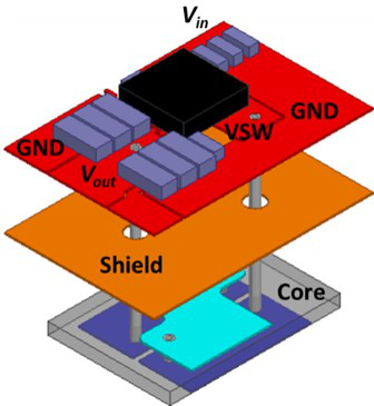
3 power density. The laminating structure is shown in Fig. 2. The bottom two layers of copper are used to build the winding of the inductor. The top layer of copper provides the connection between the other components of the converter. The second layer of copper is a shield, which alleviates EMI and minimize the parasitics of the active layer. Fig. 3 shows the PCB integrated POL module with and without mounted FETs and capacitors. The POL module survives after hundreds of thermal cycles, which validates the reliability and compatibility of the flake magnetic material with PCB integration. In addition, the application of the standard PCB process reduces the cost for manufacturing these integrated modules due to the easy automation and low-temperature process.
.jpg)
Fig. 1. (b) Prototype.

Fig. 2. 3D integrated POL module with PCB
embedded inductor substrate.

Fig. 3. Laminating structure of integrated POL module based on 4-layer PCB.
.jpg)
.jpg)
