


LIBRARY
Efficiency Evaluation of Two-level and Three-level Bridgless PFC Boost Rectifiers
Year: 2014
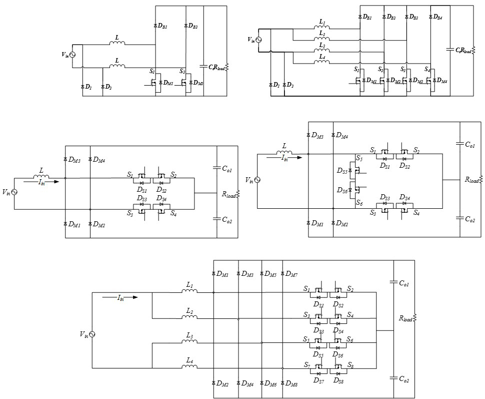
Fig. 1. (a) Semi-bridgeless PFC boost rectifier. (b) Paralleled or interleaved PFC boost rectifier. (c) Three-level bridgeless PFC boost rectifier. (d) Three-level bridgeless PFC boost rectifier with AC switch. (e) Paralleled or interleaved Three-level bridgeless PFC boost rectifier.
To estimate the efficiency of each converter, the operation of all the converters are first introduced and analyzed. Based on this, to make a fair comparison, an efficiency-oriented design optimization is conducted to all the converters. After that, the efficiency estimation is done by simulation and mathematical calculation. To be more specific, the conducting current at any time through any components can be obtained using simulation based on which the conduction loss can be calculated taking into consideration such factors as temperature. To estimate the switching loss of the switches, a piecewise linear model for MOSFET is applied. In this model, the gate charges of the MOSFET instead of the non-linear capacitance are used to calculate the turn-on and turn-off time due to the consistency of the charges in a wide voltage range. The loop inductors and the loss caused by charging the diode when turning on the switch is considered. Transition of the drain-to-source current and voltage are assumed to be linear. The efficiency comparison of the topologies is shown in Fig.2.
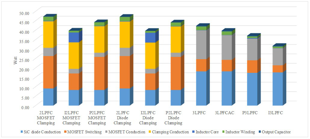
Fig. 2. Loss breakdowns of the compared topologies.
