


LIBRARY
Evaluation of High-Voltage Cascode GaN HEMT in Different Packages
Year: 2014
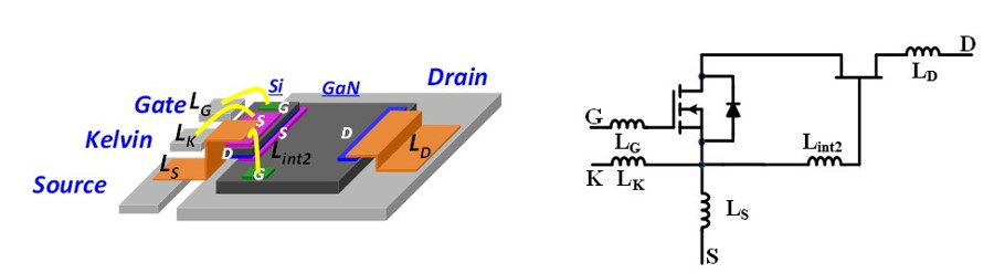
Fig. 1. Bonding diagram and schematic for cascode GaN HEMT in stack-die package.
The limitations of the traditional packaging for high-voltage cascode GaN HEMT includes significant turn-on loss during hard-switching turn-on, and significant internal parasitic ringing in hard-switching turn-off due to the impact of common-source inductors.
In order to improve the package design, we propose a stack-die package, with all common-source inductors eliminated. According to previously developed loss models, the stack-die package is predicted to have significant improvement compared to traditional packages. Experiments with a prototype of this stack-die package that was fabricated in the lab show that around 30% of the turn-on energy is reduced during hard-switching turn-on, and the internal parasitic ringing is almost eliminated in hard-switching turn-off.
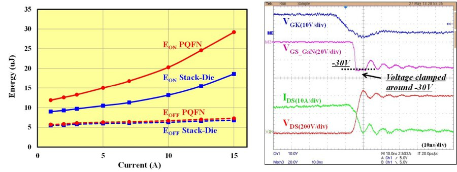
Fig. 2. Package impact in hard-switching turn-on and hard-switching turn-off.
