LIBRARY
Characterization of 650 V enhancement mode GaN HEMT

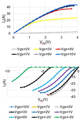
The static characterization results show that the device has an on-resistance of 55 mω at 9 A drain current and 7 V gate to-source voltage. The transistor package also has a separate source-sense pad to keep the gate to source loop independent of the drain-source loop, as shown in Fig. 1. The blocking capability of the device is also tested, and the blocking voltage is found to be 650 V with a leakage current of 2.4 µA at 25 C. The reverse characteristics (as shown in Fig. 2) are similar to that of a MOSFET with a body diode, but the GaN HEMT has no intrinsic body diode; the junction conducts during the off-state. The on-state reverse characteristics are similar to the on-state forward characteristics.
From these measurements, the on-resistance at 9 A drain current and 7 V gate to source voltage during reverse conduction is found to be 54.5 mω. The on-resistance during forward and reverse conduction at 100 C is found to be 136 mω with similar operating conductions. The transconductance is found to be 15 S at 25 C and 7.95 S at 100 C. In conclusion, by reviewing the output characteristics, the recommended on state gate to source voltage should be between 6-10 V.


