


LIBRARY
Temperature dependence of GaN MOS capacitor characteristics
Year: 2016
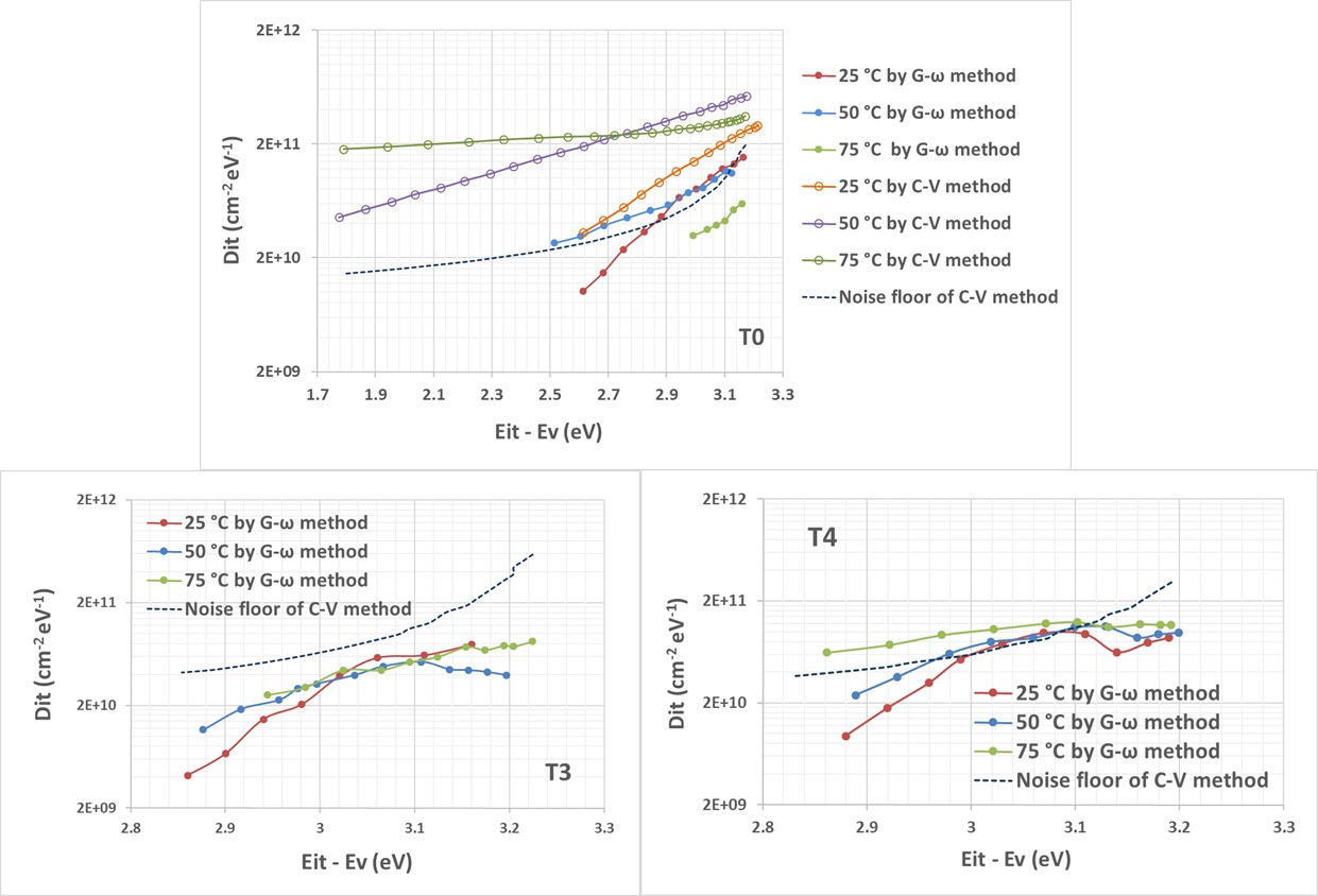
Fig. 1. Dit vs. trap energy level for T0, T3 and T4 at different temperatures
Three capacitor samples (T0, T3 and T4) were fabricated on GaN-on-sapphire substrates. No surface etch was performed on sample T0. The surfaces of T3 and T4 were dry-etched by ICP-RIE to a depth of 50 nm. Subsequently, dry etch damage was removed by a TMAH wet treatment on T3 and a NaOH wet treatment on T4. PE-TEOS SiO2 was used as a gate dielectric (1000°C anneal). AC capacitance (C-V) and conductance (G-V) measurements were performed at 25, 50 and 75°C using a HP4284A precision LCR meter. By performing a Gaussian fit of the normalized parallel conductance (Gp/ω) data (calculated from C-V and G-V curves), Dit, surface potential fluctuation (σs), trap time constant () and capture cross-section (c) of interface traps can be extracted.
Fig. 1 shows that for all three samples, the extracted apparent interface trap density (Dit) at deeper energy levels increases with increasing temperature. This is due to faster capture/emission, or equivalently the decrease of trap time constant (). A larger number of deep traps become active at higher temperature and contribute to observed Dit. Note that only for sample T0 were C-V method Dit values above the noise floor. It is clearly illustrated in Fig. 2 that decreases with increasing temperature, and increases at deeper trap levels. The decrease in at a higher temperature means that traps respond at higher frequencies. The larger trap time constant of T3 and T4 over T0 indicates the presence of different types of interface traps caused either by different material quality or by different GaN surface preparation. In addition, the capture cross section increases with temperature, which is mostly from the large reduction of trap time constant. At higher temperatures, surface potential fluctuations (σs) also increase at deeper trap levels, which is contributed by activated deeper trap levels.
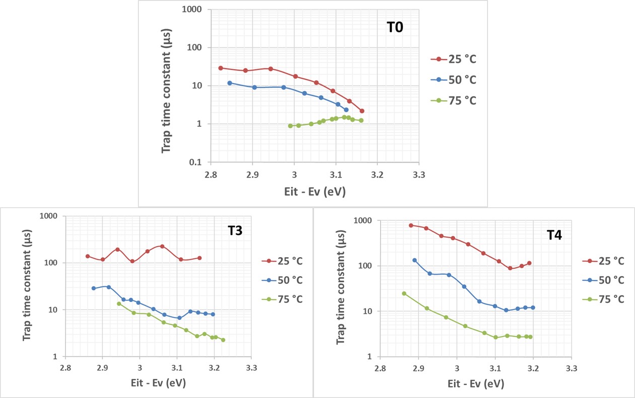
Fig. 2. vs. trap energy level for T0, T3 and T4 at different temperatures
