


LIBRARY
Testing the Switching Capability of a Normally-off 800 V - 2 A Vertical GaN Power Transistor
Year: 2017 | Author: Amy Romero | Paper: D3.1
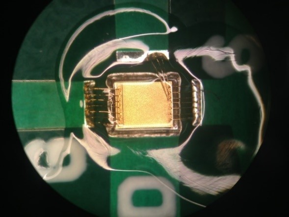
Fig. 1 Vertical GaN device after being encapsulated on PCB
The bare die of the device is subjected to these tests after being mounted onto a PCB and then wire bonded to it and encapsulated. The final encapsulated stage of the transistor can be seen in Fig. 1.
To initially characterize the device, a basic static characterization is performed using Agilent's B1505A Curve Tracer. These tests consist of transfer characteristics, output characteristics and on-state resistance over current. For the double pulse test used to assess the switching of the device, the gate to source voltage is driven from 0 V to 10 V and a 10 Ω external gate resistor is used. The switching waveforms of the device at a drain to source voltage of 400 V and a load current of 2 A are shown in Fig. 2 and Fig. 3. These waveforms are used to calculate the switching losses and switching on times.
These results show the potential that a vertical GaN device has in the push to find a replacement for silicon that has better performance with a lower price. Further testing objectives are to decrease the external gate resistor used for the switching test and to test the device at higher voltages.
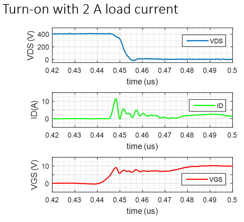
Fig. 2. Turn-on waveforms with a load current of 2 A at a VDS of 400 V
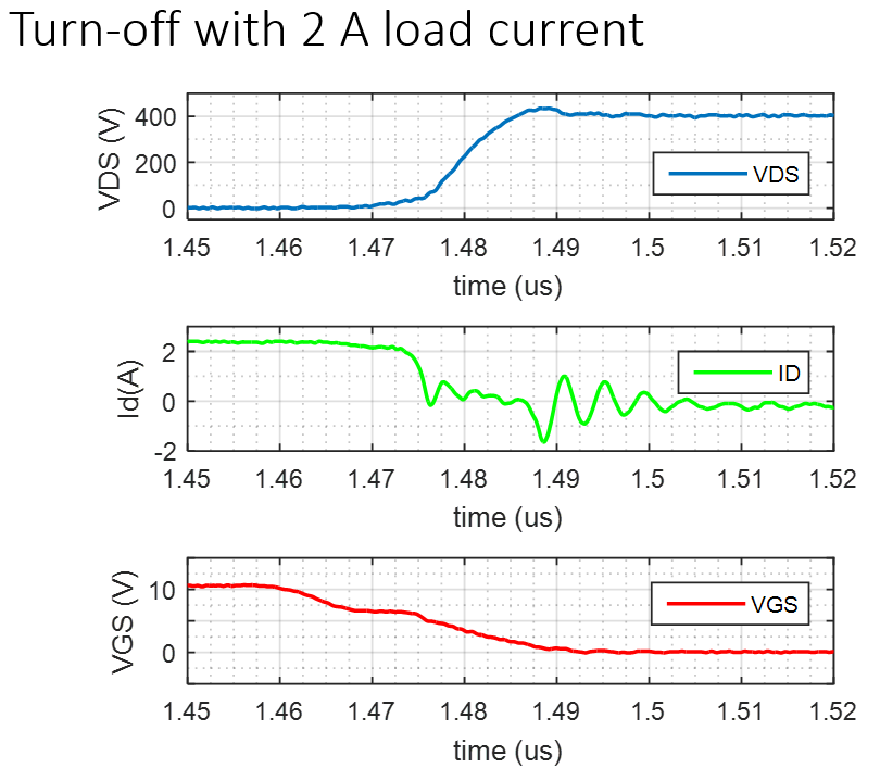
Fig. 3. Turn-off waveforms with a load current of 2 A at a VDS of 400 V.
