LIBRARY
Loss Model and Optimization Method for a Switched-Capacitor Divider for a POL Application

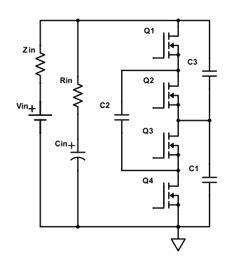
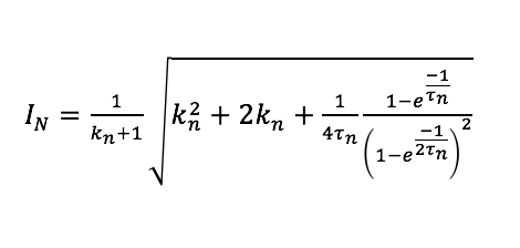
Fig. 1 shows the schematic of a 2:1 switched-capacitor divider. Eq. 1 shows the 2:1 voltage divider rms current based on the ratio of C2/(C1+C3), kn and the normalized time constant of the circuit (τnn = τ/T). The time constant of the circuit is related to the chosen device, and the total capacitance used, in the circuit. This paper finds the model matches closely with the simulation, and the results are within a 5 percent comparative range.
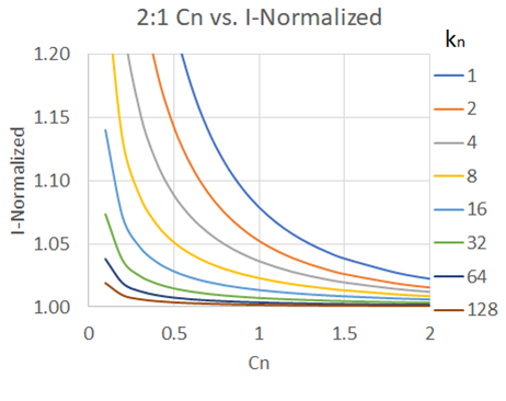
The time constant of a switched-capacitor divider is closely related to the total capacitance used in the circuit. Using this relationship, the tradeoffs between efficiency (conduction loss is the major loss at high load condition) and the total capacitance used for a given device and frequency can be determined, as shown in Fig. 2. By using the same amount of total capacitance, a switched-capacitor divider circuit can achieve higher efficiency by changing the capacitance ratio between C2 and the output capacitors. However, choosing the highest kn is not necessarily desirable. Due to the higher peak on C2 current that may affect the electromagnetic interference performance of the circuit, the noise may get coupled to the output, due to the high peak current, affecting the performance of the processor in POL applications.


