LIBRARY
Power Supply with Low Input-Output Capacitance for Multiple Gate Driver Units of a 10 kV SiC-MOSFET Module
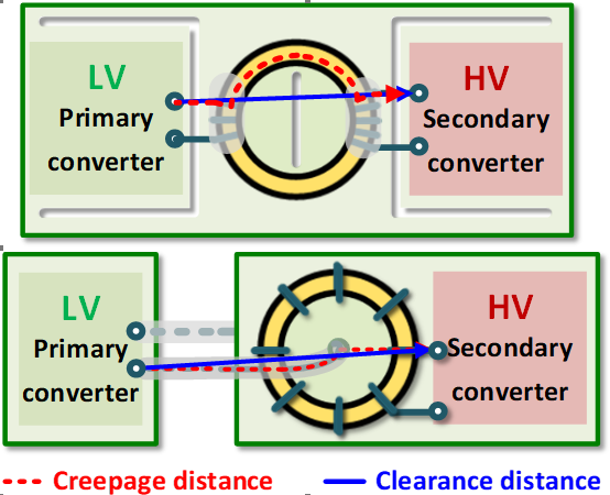
To satisfy the critical creepage and clearance distance requirements, conventional designs use a magnetic core to isolate the primary and secondary windings. The result is a large and heavy circuit. In order to reduce the size, a transformer design approach with a single turn at the primary side is proposed. With this approach, the primary side winding becomes a conducting wire across the core, allowing its interfaces to be removed to another board, and the primary HV cable length to be utilized as part of the creepage path (see Fig.1.). The HV insulation is also simplified when using the HV insulation material around the cable.
In terms of the low CI/O design, four optimization parameters are considered. The parameters are inner core radius Ri, core height lh, wire diameter dw, and secondary turn number Ns. The CI/O is calculated by using the stored electric energy method and is verified by the measurement. CI/O increases with the growth of lh, dw, and Ns while it decreases with the growth of Ri.
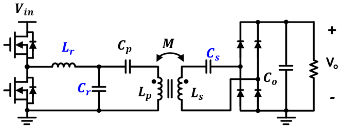
The LCCL-LC resonant converter is considered as it presents current source characteristics at the primary side. It achieves load-independence, and eliminates the impact of leakage inductance. The converter specifications are shown as Vin = 24 V, Vo = 28 V, Po = 10 W.
In terms of switch selection, gallium-nitride devices are considered because of their proven performance at high-frequency ranges. EPC 2104 is chosen since it has the lowest losses due to small on-resistance (Rds_on) and output capacitance (Coss). Finally, the gate driver uses the high-integrated chip, model number LM5113, manufactured by Texas Instruments.
