


LIBRARY
PCB-Interposer-on-DBC Packaging of 650 V, 120 A GaN HEMTs
Year: 2020 | Author: Shengchang Lu | Paper: T1.11
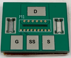
Fig. 1. The front view of the GaN HEMT package.
To achieve small package parasitic inductances and a large foot- print ratio, many have taken the approach of embedding bare die into printed circuit boards (PCBs). One version of this PCB approach requires a 5-10 ?m copper finish on the device, not a standard process in die fabrication. And, to protect the die surface, an extra buffer layer is required to avoid damaging the die surface when using UV laser drilling holes in the PCB. Other versions of the approach use mechanical drilling to create channels in the die surface and rely on stud bump or a foam interposer for the PCB-to-die interconnection. These versions are not effective for heat dissipation. Yet another version uses a four-layer PCB with die buried between the second and third copper layer and the devices thermal pad connected to the bottom copper layer. This one has a larger junction-to-case thermal resistance and a lower thermo-mechanical reliability due to a large CTE mismatch between the PCB and GaN die.
This paper introduces an alternative packaging approach that
combines a PCB interposer for device interconnection and a DBC substrate for heat dissipation, electrical isolation and lower CTE mismatch. To achieve low parasitic inductances, the bare dies gate, drain, and source pads were connected directly to the PCB interposer via gold-plated pins. The footprint of the packaged device is similar to that of the bare die. Gate drivers and other driver components can also be surface-mounted on the PCB. To improve heat extraction and provide electrical isolation from devices substrate to heat sink, we used an AlN DBC substrate and silver sintering for die-attach and pin connections. To ensure the mechanical robustness of the package, we applied underfills between the PCB and DBC. The front view of the package is shown in Fig. 1, and the cross-section view is shown in Fig. 2.
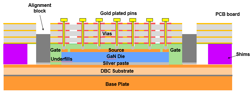
Fig. 2. The cross-section view of the GaN HEMT package.
