


LIBRARY
Packaging and High-Temperature Characterization of a 650 V, 150 A eGaN HEMT
Year: 2021 | Author: Shengchang Lu | Paper: S5.3
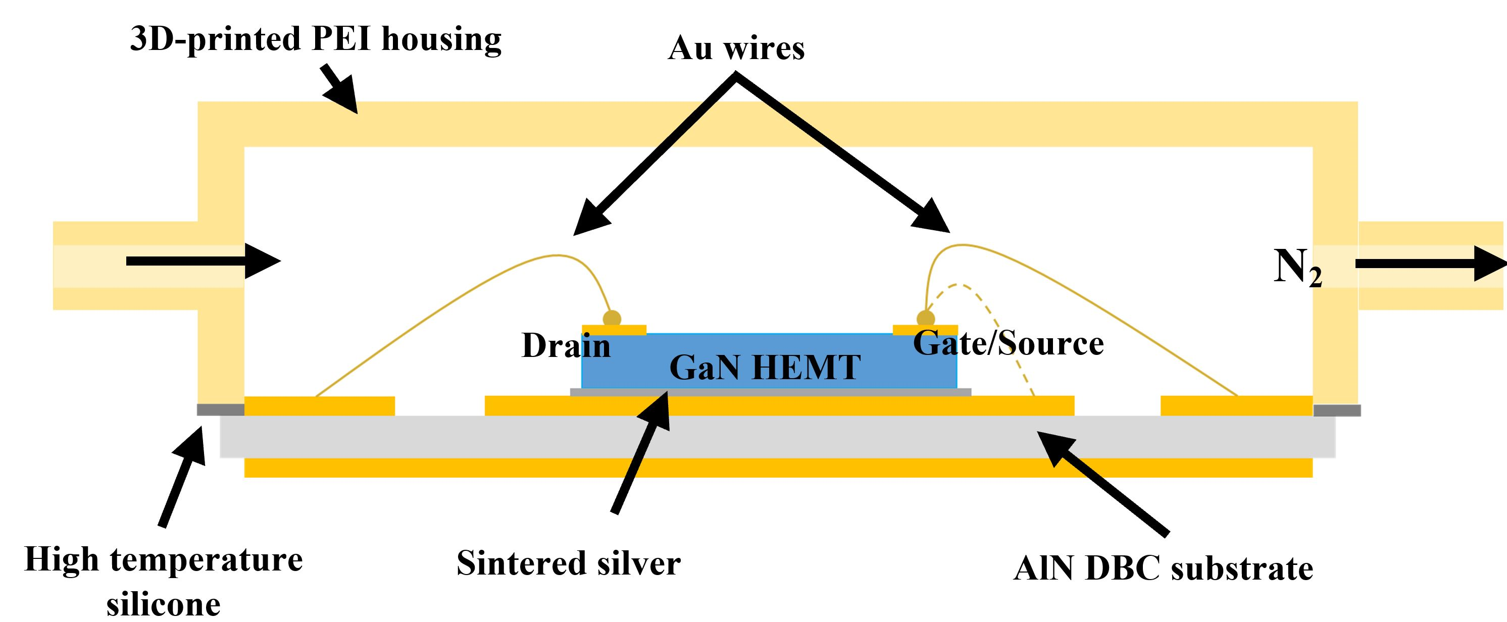
Fig. 1. Cross-sectional schematic of the high-temperature package for interconnecting and enclosing the eGaN HEMT.
In this work, a commercial 650 V, 150 A enchancement mode GaN (eGaN) HEMT from GaN Systems was packaged and characterized for its static properties at temperatures up to 250° C. The eGaN HEMTs studied in this work were purchased from GaN Systems with the part number of GS-065-150-1-D rated at 650 V, 150 A. Copper was the surface finish on all the gate, source, and drain pads, and the backside of the chip was finished with silver.
Fig. 1 is a cross-sectional view of the package design. Silver sintering was used for attaching the device chip on direct-bond-copper substrate, and gold wire-bonding for interconnections. Fig. 2 shows the fabrication process of the high-temperature package.
The packaged device was tested at temperatures up to 250 ° C to determine the effects of temperature on its static characteristics. It survived multiple heating/cooling cycles between room temperature and 250° C as it underwent static testing on a curve tracer. Compared to the characteristics at room temperature, at 250 ° C, the threshold voltage was reduced by about 30%, the saturation current was down below 45% of the rated current, and the leakage current was increased by tens of times.
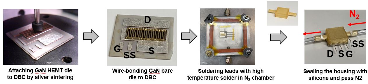
Fig. 2. Fabrication steps of the high-temperature package.
