


NEWS
CPES Researchers Win the 2023 IEEE EDS George E. Smith Award!
May 14, 2024
CPES Researchers win the 2023 IEEE EDS George E. Smith Award!
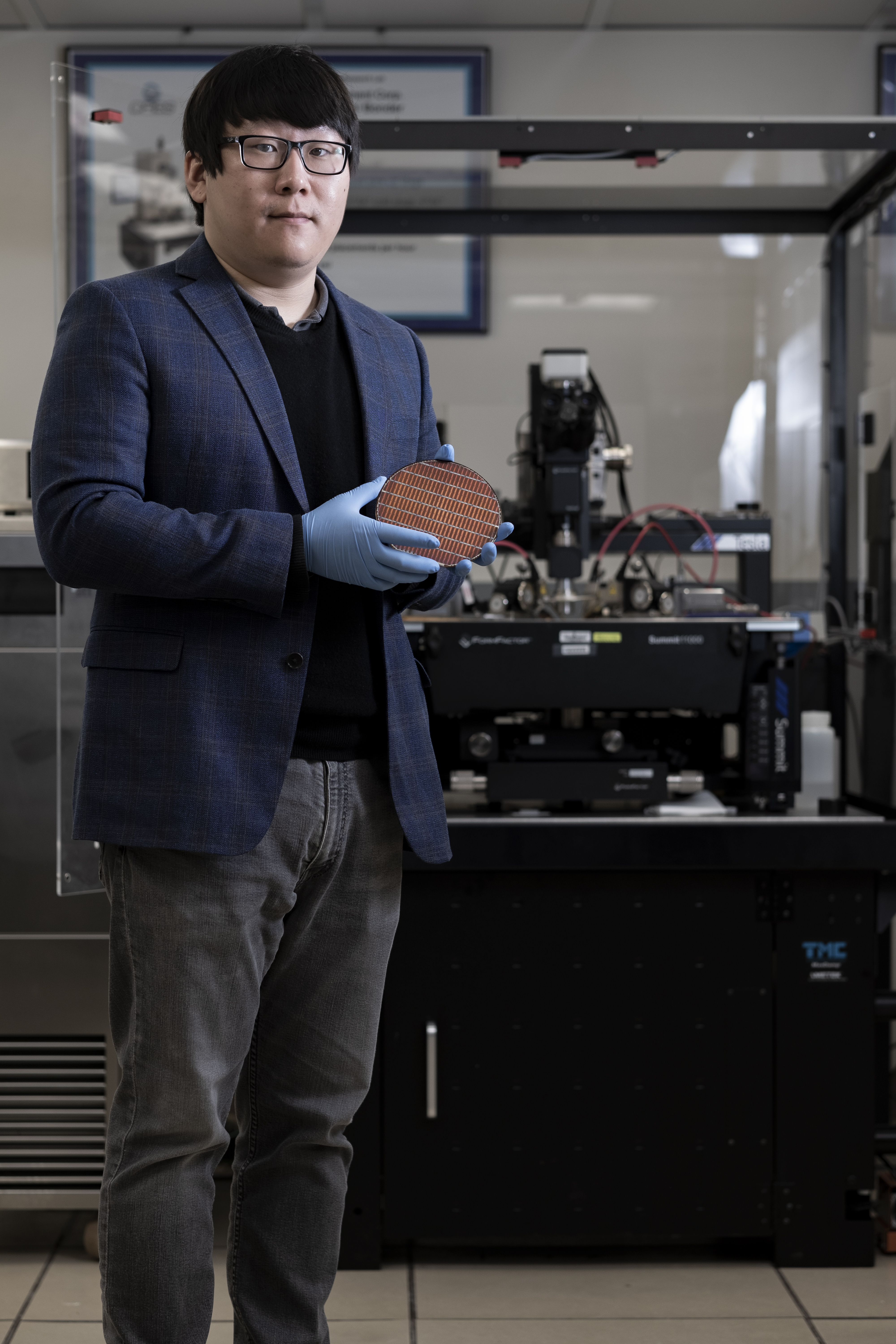
Ming Xiao is lead author on the paper which won the 2023 IEEE EDS George E. Smith Award.
“Robust Avalanche in 1.7 kV Vertical GaN Diodes with a Single-Implant Bevel Edge Termination” is available through IEEE at this link.
The article appeared in the October 2023 issue of Electron Device Letters (EDL) and was selected by the IEEE Electron Devices Society from almost 500 papers published in the journal in 2023. This prestigious award signifies a strong endorsement of the high quality of the research being reported.
Co-authors are Yifan Wang, Ruizhe Zhang, Qihao Song, Matthew Porter, Eric Carlson, Kai Cheng, Khai Ngo and Yuhao Zhang.
The award will be presented at the IEEE International Electron Devices Meeting (IEDM) in San Francisco, CA.
Congratulations to all authors!
Citation & Abstract
M. Xiao et al., "Robust Avalanche in 1.7 kV Vertical GaN Diodes With a Single-Implant Bevel Edge Termination," in IEEE Electron Device Letters, vol. 44, no. 10, pp. 1616-1619, Oct. 2023, doi: 10.1109/LED.2023.3302312.
This work demonstrates a novel junction termination extension (JTE) with a graded charge profile for vertical GaN p-n diodes. The fabrication of this JTE obviates GaN etch and requires only a single-step implantation. A bi-layer photoresist is used to produce an ultra-small bevel angle (~0.1o) at the sidewall of a dielectric layer. This tapered dielectric layer is then used as the implantation mask to produce a graded charge profile in p-GaN. The fabricated GaN p-n diodes show a breakdown voltage (BV) of 1.7 kV (83% of the parallel-plane limit) with positive temperature coefficient, as well as a high avalanche current density over 1100 A/cm2 at BV in the unclamped inductive switching test. This robust avalanche is ascribed to the migration of the major impact ionization location from the JTE edge to the main junction. This single-implant, efficient, avalanche-capable JTE can potentially become a building block of many vertical GaN devices, and its fabrication technique has wide device and material applicability.
