RESEARCH
Tri-gate GaN Junction High-Electron-Mobility Transistors

A self-aligned process is used to deposit the NiO and gate metal in the same lithography step. The NiO is deposited in a magnetron sputtering system using the NiO target. Fig.1 shows the scanning electron microscopy (SEM) images of the GaN fins before and after NiO sputtering, verifying the conformal NiO coverage. A hole concentration and mobility of 5×1019 cm-3 and 0.7 cm2/V3, respectively, are extracted for the sputtered p-NiO. For the tri-gate MISHEMTs.
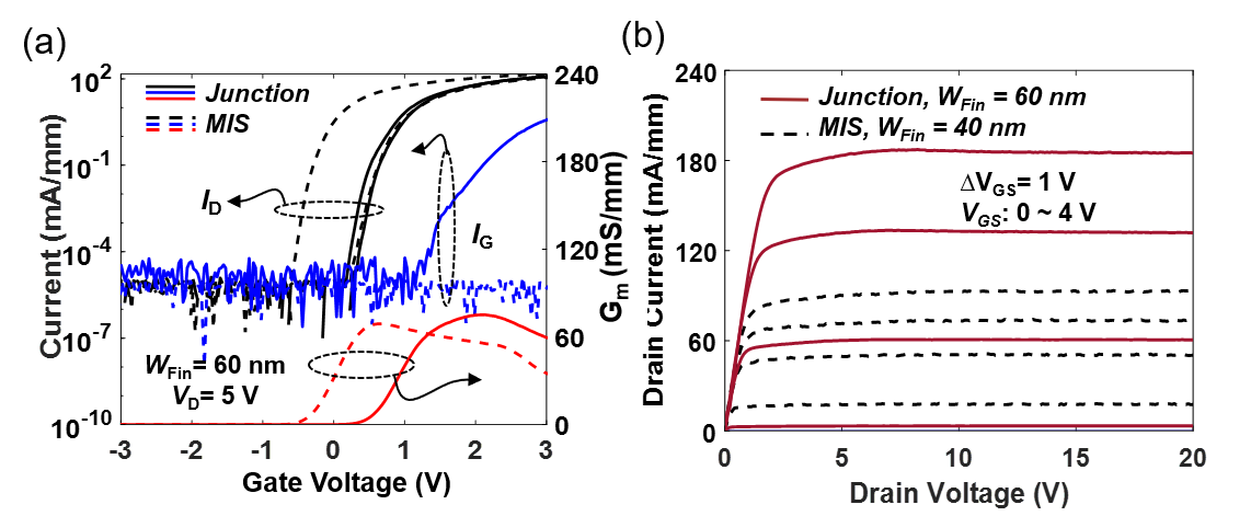
Fig. 2(a) shows the double-sweep transfer characteristics (VDS = 5 V, saturation region) of the tri-gate JHEMTs and MISHEMTs with 60 nm WFin. The tri-gate JHEMT has a VTH of 0.45 V (extracted at 1 μA/mm drain current) and
a hysteresis below 0.1 V, while the tri-gate MISHEMTs show a negative VTH and ~0.6 V hysteresis. The close- to-60 mV/decade SS and small hysteresis in tri-gate JHEMTs suggest very small interface states in NiO-based junction gate. The tri-gate JHEMT faces larger gate leakage current when NiO/2DEG diode turns on. Fig. 2(b) shows the output characteristics of the 60-nm tri-gate JHEMTs and 40-nm tri-gate MISHEMTs with a similar VTH . The higher current density in the tri-gate JHEMT is mainly due to the larger portion of the gate for current conduction.
