RESEARCH
Optimization of Electric-Field Grading Plates in a PCB-Integrated Bus Bar for a High-Density 10 kV SiC MOSFET Power Module

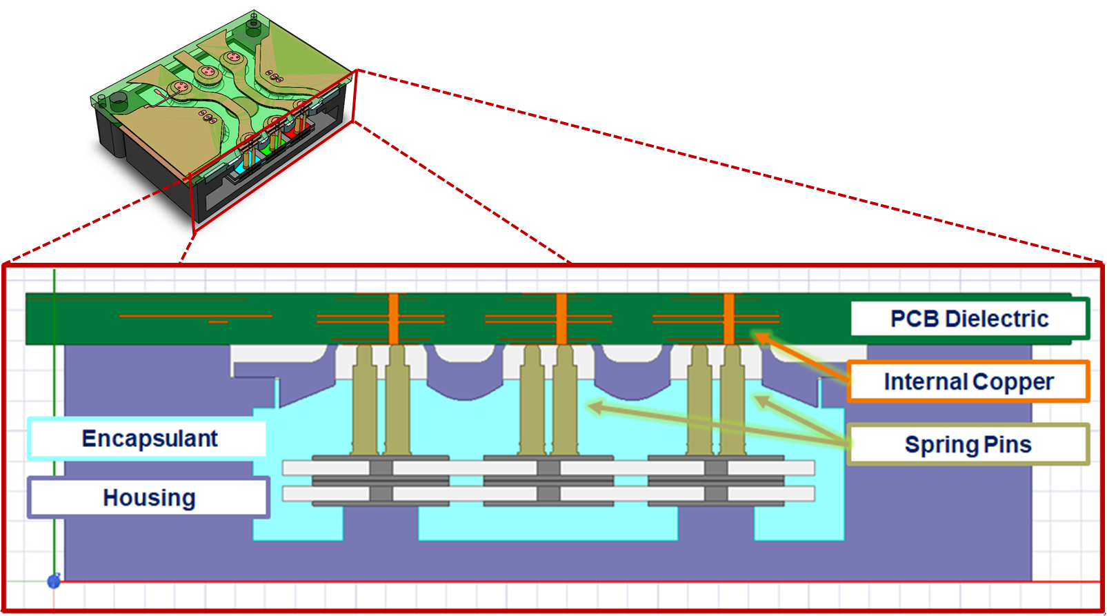
To reduce the electric field strength in the air surrounding the interface, copper traces inside the PCB are used as field- grading plates that shift the peak electric field from the air to the FR4 dielectric, which has a higher breakdown field strength than air. The geometry and location of the field- grading plates is critical to their effectiveness. To design the geometry, a numerical optimization technique is used in conjunction with finite element analysis (FEA). The system is first decomposed into critical 2D design regions, which are then parameterized, and the locations of field crowding are identified. A weighted cost function is formulated using the breakdown strength of the materials and optimized using an interior-point algorithm with finite difference derivatives.
One of these optimized cross-sections is shown in Fig.2. The optimization results in copper conductor shapes that contain the high electric field strength in the FR4 dielectric, where the field can be supported without partial discharge. Meanwhile, the electric field in air is kept below the breakdown strength of air, resulting in safe, reliable, partial-discharge-free operation. The optimized laminate bus bar and optimized module housing were built and experimentally demonstrated a partial discharge inception voltage of 11.6 kV rms (16.4 kV peak) under 60Hz sinusoidal excitation.


