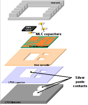
Fig. 1. Conceptual Structure of CPES 3D Integrated Power Supply.
The integrated power supply research is conducted by a multi-disciplinary team with materials, packaging, semiconductor devices and circuits, together with system-level expertise to develop an integrated approach, where ultimately power supply could be integrated with microprocessors or other applications. One of the key steps towards integration of power supply with a given load is to first integrate power supply in a three-dimensional integration of active components as well as passive components into a common structure. CPES researchers have developed a packaging approach, here referred to as "stacked power." It allows for active components to be embedded inside ceramic layers with high thermal conductivity. This structure frees up the top and bottom sides for the integration of other parts of the circuit, including passive components such as inductors and capacitors, as well as other active components, such as drivers, sensors, and controllers. This vertical integration allows for layouts with low circuit parasitics so that efficient high-frequency operation can be realized. High-operating frequency reduces the size of the passive components needed, thus increasing power density. This then will help facilitate the ultimate integration of power supply with its intended load. The stacked layers are made using Direct Bonded Copper (DBC) which integrates the thermal management into the package as well. This further reduces cost by eliminating the need for a heat sink when used with a modest airflow. The passives are integrated with the active layer by means of low-temperature co-fired ceramics (LTCC). LTCC technology enables the integration of low-profile inductors as well as capacitors in a package that could easily be integrated with active components, as mentioned above.
A single-phase module with combined active and LTCC passive layers has been tested and achieved 83% efficiency at 18A output current and 91% at a light load of 4.5A -- all this with a very high power density of 127 W/in
3. This good light-load efficiency will be a huge benefit for reduction of power consumption for computer related applications where the light load operation is very common. Stacked Power achieves small size and high power capability while saving energy -- which is something we can all appreciate.

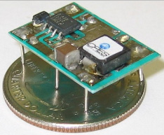
Fig. 2. Photo of integrated active layer on a coin.
