RESEARCH
Characterizations and Modeling of SiC JFET
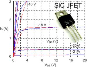
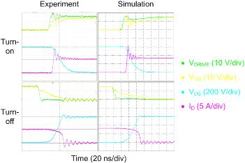
(Blue solid - measurement; red dashed - simulation).
CPES has been spending a lot of efforts in investigating the performances of the new SiC JFETs. Extensive measurements and tests have been recently conducted on 1.2 kV, 5 A prototype SiC JFETs manufactured by SiCED. Static characteristics, including the output and transfer characteristics, on-state resistances, gate and body diodes, as well as junction capacitances, etc, were all obtained with the use of the curve tracer and the impedance analyzer. The switching performances of the device, on the other hand, were tested on a self-built double-pulse tester with minimized PCB stray inductances in order to reduce the circuit parasitic impact on the device's switching characteristics. With this tester, the SiC JFET was able to switch with zero gate resistance, causing only minor ringing during the fast switching transients. Under 600 V, 6 A inductive load switching condition, the device dv/dt rate could reach 60 kV/us and di/dt rate could reach 3 kA/us.
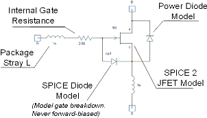
The characterization data were directly used to build the device model based on the SPICE-2 JFET model. Extra components were added to the SPICE-2 model to take into account the particularities of the SiC JFET. As an example, an extra SPICE diode was added to the gate-source terminals in order to capture the gate breakdown of the JFET when this feature is intentionally used in the gate driving strategy. The model was verified by comparing simulation waveforms with experimental results obtained in the switching tests, and now is being used in the SiC JFET phase-leg and converter design in CPES.
