RESEARCH
Characterizations and Modeling of SiC MOSFET

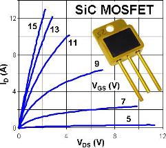
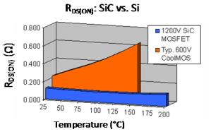
CPES has conducted extensive characterization and testing work on SiC MOSFETs. A full static and switching characterization process has been carried out recently on a 1.2 kV, 20 A prototype device manufactured by CREE. The static characteristics, such as output characteristics, body diode I-V curve, internal gate resistance, as well as junction capacitances and package stray inductances, have all been obtained with the use of the curve tracer and the impedance analyzer. All these characterizations have also been repeated under different temperatures from 25 to 200°C in order to evaluate the influence of the temperature. A 5 to 8 times reduction in RDS(ON) has been observed for this device, compared to the conventional Si CoolMOS with similar current ratings (See Fig. 2). The switching performances of the device, on the other hand, have been tested on a self-built double-pulse tester with minimized PCB stray inductances in order to reduce the circuit parasitic impact on the device's switching behavior. Characteristics such as switching times and losses, voltage / current overshoots and ringing, etc, have all been investigated in the test. With this tester, the SiC MOSFET can be switched at a dv/dt rate of 20 kV/us and di/dt rate of 2 kA/us, without causing unacceptable ringing during switching transients.
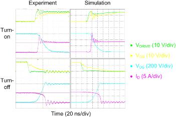
With the characterization data, the SiC MOSFET model can be built with the use of Power MOSFET Tool in Synopsys Saber, a modeling tool which takes into consideration all the important static and dynamic characteristics of the device. The model parameters were extracted by curve-fitting the measurement data in the program. The obtained MOSFET model has been verified by comparing simulation with experimental switching waveforms and great accuracy has been achieved (See Fig. 3). The characterization and modeling processes are generic so that they can be applied to studying any new SiC MOSFETs.


