RESEARCH
Performance Projection of Vertical High-Voltage GaN power MOSFETs and Comparison to SiC power MOSFETs

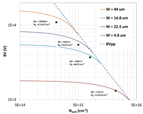
Fig. 1 shows the calculated punch-through breakdown voltage curves for GaN at different drift layer thicknesses corresponding to the drift layer thickness used at different voltage ratings. The drift region doping and thickness is optimized to obtain the lowest drift region resistance for a given blocking voltage (highlighted by markers in Figure 1). Channel length values of 1 µm and 0.5 µm are simulated. Channel mobility of 100 cm2/V.s and an oxide thickness of 50 nm is used. Fig. 2 shows the extracted specific on resistance of the devices as a function of blocking voltage compared with the reported values for the 4H-SiC MOSFETs. A resistive switching simulation is performed with Jon = 100 A/cm2, VDD = rated BV. The extracted performance metrics of the GaN MOSFETs are listed in the table below. The GaN MOSFETs give a much lower on-resistance than commercially available 4H-SiC MOSFETs at all BV ratings. These simulations quantify the significant performance benefits that can be achieved by vertical GaN power devices for high frequency applications as compared to 4H-SiC power devices.


