RESEARCH
MHz LLC Resonant Converter Design with Planar Matrix Transformer for Telecom Application

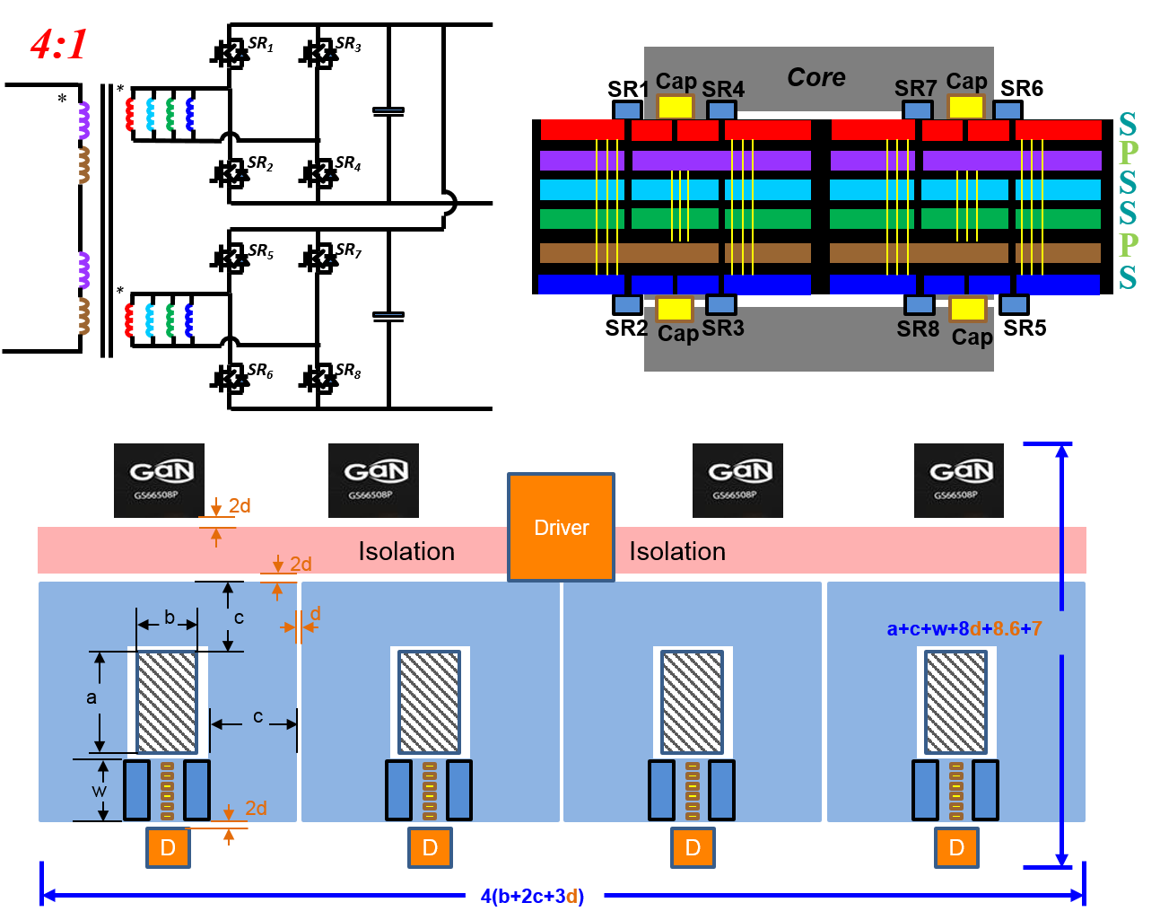
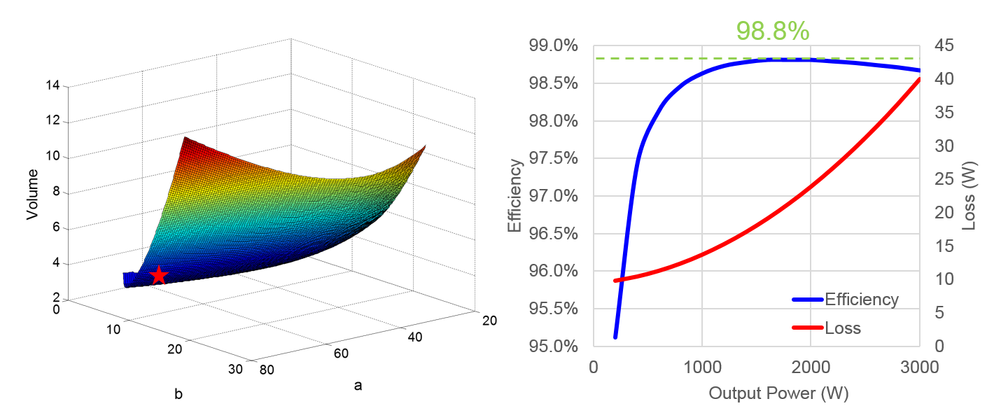
A design procedure for the secondary DC/DC stage is proposed. First, the secondary side topology is chosen from among a full bridge rectifier, voltage doubler, and center tap, according to the tradeoff between device number, device stress, core loss, and winding loss. Second, the primary side and secondary side of the device are selected according to the breakdown voltage, Rdson and Qg, which represent its conduction loss and switching loss respectively. Third, in order to get a low profile, and easily manufacture the converter, a multi-layer PCB winding based planar transformer is used, as shown in Figure 1. This winding structure takes into consideration interleaving between windings as well as termination between windings and synchronous rectification devices, and helps to minimize the AC winding loss due to proximity and skin effect, which is dominant over DC winding loss in high frequency applications. Fourth, an analytical transformer loss model is constructed based on three kinds of transformer loss: 1) Winding loss. 2) Core loss and 3) Termination loss. The Dowell Equation and Modified Steinmetz-Equation are adopted to calculate the winding loss and core loss respectively, and 3D FEA simulation is used to determine the termination loss. This analytical transformer loss model is verified by 3D FEA simulation. With this loss model, much simulation time can be saved and an optimized transformer design with the lowest loss and volume is accomplished, as shown in Figure 2, which also shows the predicted efficiency curve.


