RESEARCH
A Novel High Efficiency System Architecture for Bi-directional On Board Battery Charger
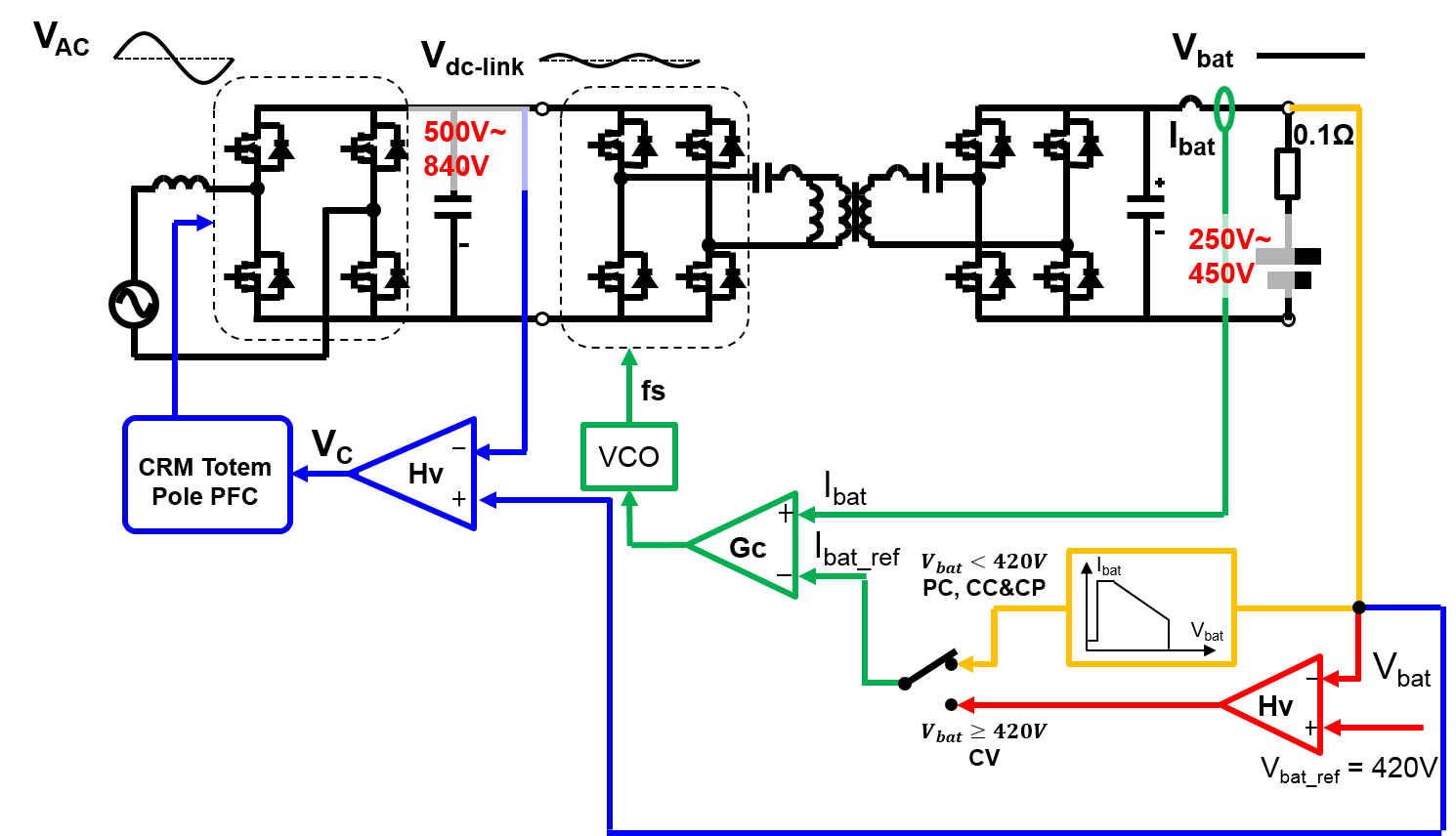
In order to make the CLLC resonant converter working at its optimized point, two different candidate structures are evaluated and compared in terms of efficiency: conventional fixed 400V DC-link voltage using GaN devices and variable 500V-840V DC-link voltage with mixed wide band gap devices, as shown in Fig. 1. It is shown that the latter candidate has the smallest gain range, as shown in Fig. 2, resulting in smaller frequency range and lower loss. In order to handle the high DC-link voltage, 1.2kV SiC devices are used in PFC stage and the primary side of the DC/DC stage. 650V GaN devices are used as secondary side synchronize rectifier. In addition, a two stage combined control strategy is proposed, as shown in Fig. 1. The blue line shows the PFC stage control, which is responsible to keep the average DC-link voltage tracking battery voltage. The green line is to control the switching frequency of the CLLC resonant converter. The red and yellow line is a non-linear function to determine the battery charging stage. By using this proposed structure, the switching frequency of the resonant converter is always kept around resonant frequency, which gives the best efficiency.
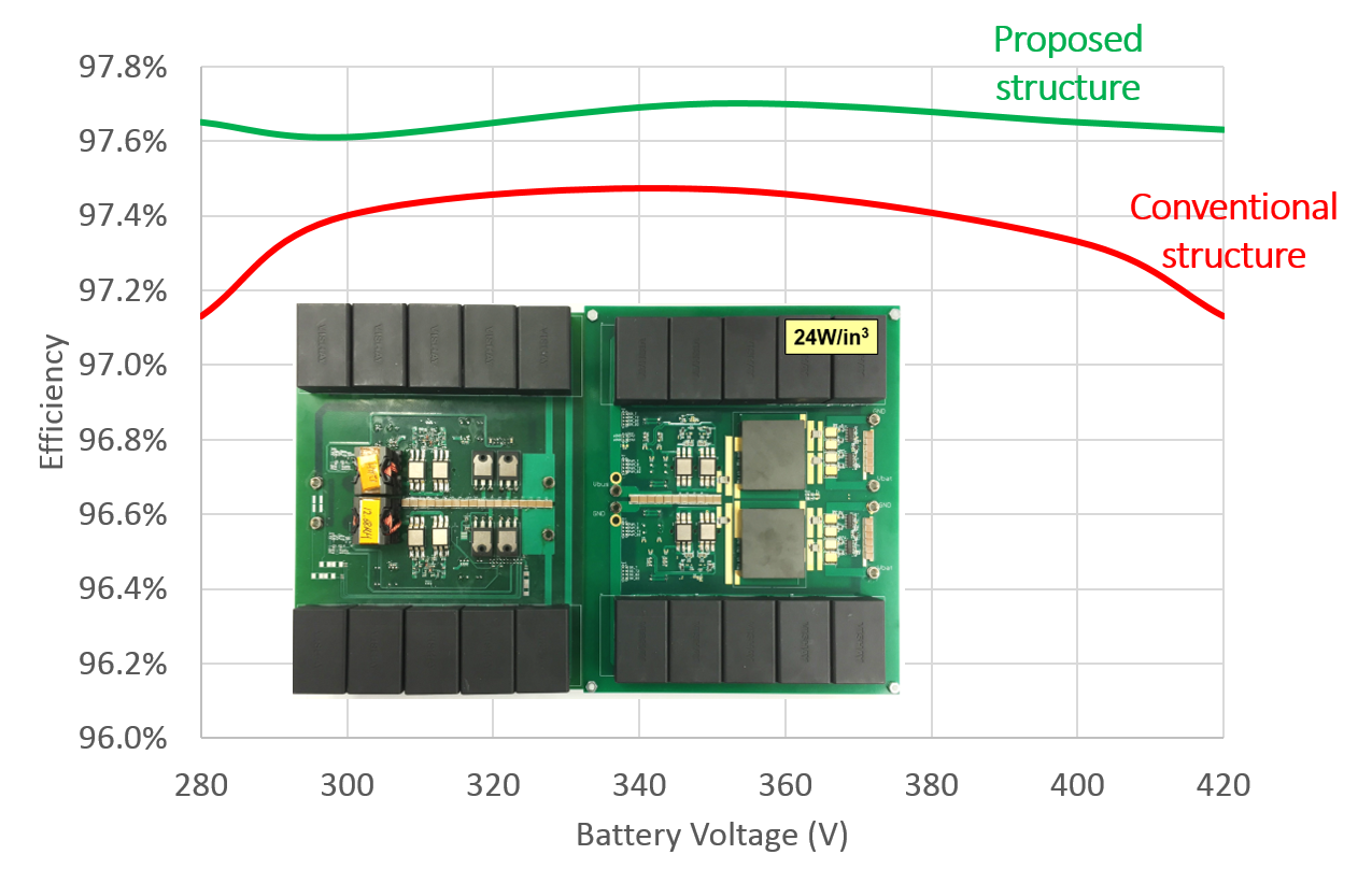
A 6.6kW 500kHz prototype is built to verify the proposed two stage system structure and control strategy. The efficiency results are shown in Fig. 3 as well as the hardware, which uses PCB winding transformer with leakage integration. 97.6% efficiency can be achieved over the whole battery voltage range.

