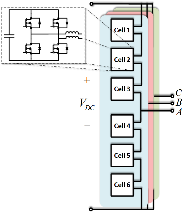
Fig. 1. Circuit configuration of a modular multilevel con-verter
The modular multilevel converter (MMC) has received increased attention over time due to its interesting features, such as inherent modularity, voltage and current scalability, and easy as-sembly. While the MMC has the advantage of having a flexible converter design, the design still requires reliability, like any other system. Modeling and simulation are powerful tools in design-ing a converter. However, a fundamental disconnect often exists between simulations and prac-tical applications. Whereas most simulations are deterministic in nature, when engineering applications are steeped in uncertainty arising from a number of sources - such as those due to the manufacturing processes, natural material variability, initial conditions, wear or damaged conditions of the system, and the system surroundings - the modeling process itself can introduce huge uncertainties. These can be due to assumptions made during the process as well as the numerical approximations employed in the simulations. Therefore, design margins are conservatively estimated using a heuristic factor of safety to compensate for the deviation of real system behavior from simulation results when using modeling and simulation in converter design.
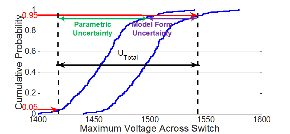
In this paper, a new approach is proposed in which different sources of uncertainties that cause the mismatch between modeling and simulation predictions and real system behavior are identified and characterized so that they can be predicted ahead of time to eliminate the use of large safety margins (shown in Fig. 2). Using this approach, modeling and simulation results can be used during the early design stages with confidence in their predictive proficiency and accuracy.
In the first section, an overview of the verification, validation, and uncertainty quantification (VV&UQ) process is described as enabling us to identify, characterize and quantify different sources of uncertainties in modeling, simulation, and experiment. In the second section, the concept from the first section is employed to calculate and minimize the required design mar-gins by using probabilistic modeling and simulation. To this end, the peak voltage across the semiconductor device in an MMC (shown in Fig. 1) - which is a key variable used to size the capacitor bank - is selected as an example to illustrate the methodology proposed in this paper.

Fig. 2. Final probability box of maximum voltage across semiconductor device indicating total uncertainty
