RESEARCH
Design Consideration of MHz Active Clamp Flyback Converter with GaN Devices for Low Power Adapter Application

Flyback converters are the dominant topology for low-power adapter applications due to their simplicity and low cost. With an active clamp circuit, the leakage energy can be recycled, and the voltage ringing minimized. Moreover, ZVS for both the main switch and the clamping switch can be realized by proper design as well. The traditional flyback transformer is hand-made, which is an intensive, labor-involved manufacturing process. The manufacturing cost is a concern, and the parameter variation is another circuit design issue. A PCB winding-based transformer is only feasible when the switching frequency is over several hundred kHz due to its capacity for fewer turns and a smaller core size. The leakage inductance and parasitic ca-pacitance of the transformer can be well-controlled by PCB manufacturers. Moreover, shielding can be easily integrated in the PCB winding to reduce the CM noise.
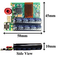
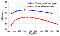
Figure 1 shows the prototype of a MHz active clamp flyback front-end converter. The size of the flyback transformer, EMI filter and output filter are significantly reduced, with 10 times high-er switching frequency than industry practice. The power density excluding the case is over 40W/in3, which is two times higher than the state-of-the-art product. The measured full load effi-ciency over a wide input range is shown in Figure 2. The efficiency of the prototype is 1~2% higher than the state-of-the-art product. It is worthwhile to point out that the power density im-provement is accompanied with efficiency improvement due to thermal restriction. Based on the thermal simulation carried on a converter which is enclosed by a case, the converter efficiency should be above 92% at worst case to achieve 25W/in3 power density without violating the thermal standard IEC60950.


