RESEARCH
A Novel WBG-Based Bi-Directional On Board Charger
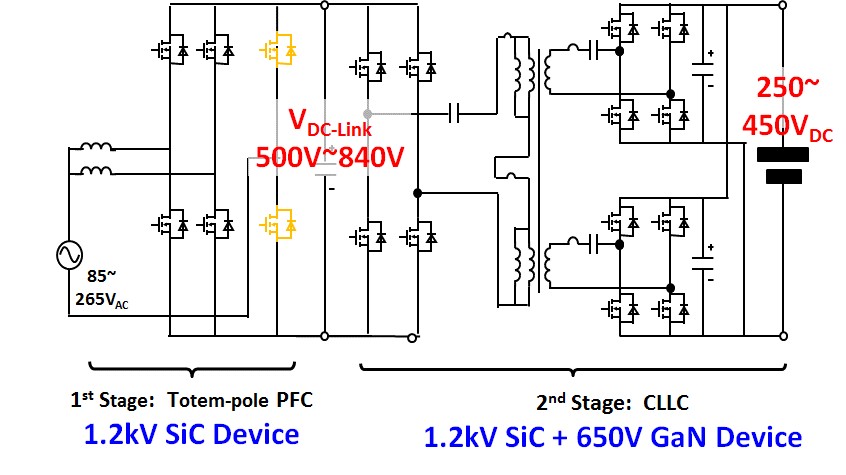
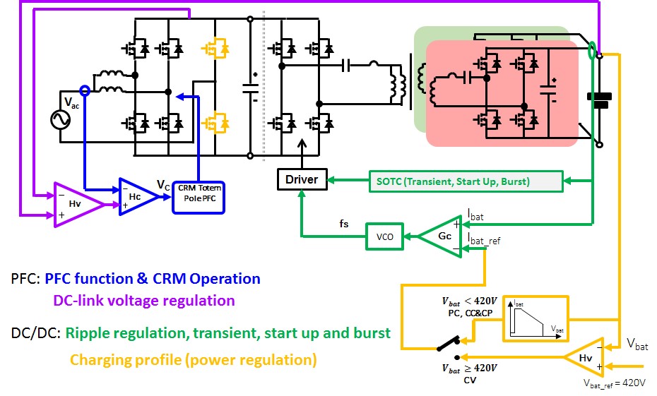
However, the large battery voltage range posts a great challenge to the design of the second stage, which is a CLLC bi-directional resonant converter. In order to guarantee the second stage working at its optimized point, four different candidate structures are evaluated and compared in terms of efficiency. Finally, a variable 500V-840V dc-link voltage with mixed wide-band-gap devices, as shown in Fig. 1 is proposed. It is shown that the proposed structure has the smallest gain range, resulting in the smallest frequency range and lowest loss. In order to handle the high dc-link voltage, 1.2kV SiC devices are used in the PFC stage and the primary side of the dc/dc stage. Since the battery voltage is still low, 650V GaN devices can be used as secondary side synchronized rectifiers.
The benefit of the proposed variable dc-link structure is to keep the switching frequency of the dc/dc stage at resonant frequency so that high efficiency can be maintained over the entire battery voltage range. This dc transformer (DCX) concept has been proved to be very efficient. However, in applications like battery chargers, this concept has the problem of a very large output current ripple.
In order to solve this problem, a two-stage combined control strategy is proposed, as shown in Fig. 2. The outer loop of the PFC stage senses the battery voltage as well as the dc-link voltage, and by using a regulator, the output power is controlled so that the dc-link voltage always tracks the battery voltage, making sure the gain range of CLLC resonant converter is close to unity. In addition, this control strategy can be extended to discharging mode, including both grid-tied mode and stand-alone load mode.
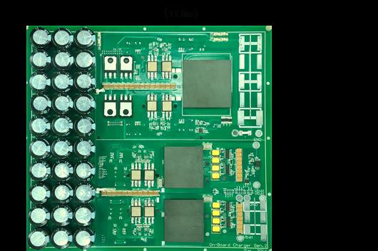
A 6.6kW 500kHz prototype is built to verify the proposed two stage system structure and control strategy as shown in Fig. 3. Over 96% total efficiency can be achieved over the entire battery voltage range with power density over 37 W/in3, which is far beyond current practice.
