RESEARCH
Insulation Design and Assessment of a 16 kV Rated PCB Based Planar DC Bus with Distributed Capacitors
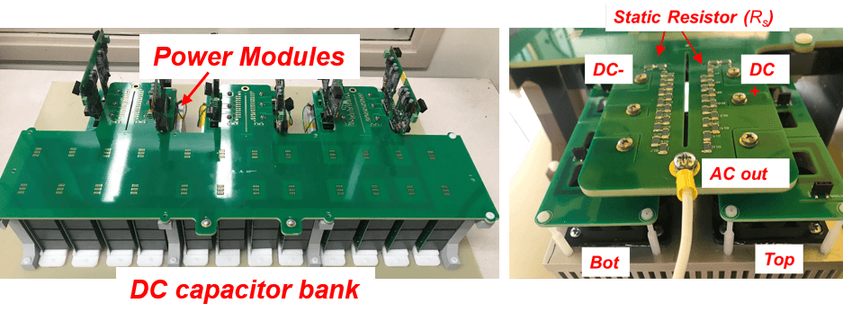
In this work, a multilayer (16 layers) PCB stack is designed for accommodating the series/parallel MV capacitor bank of a 16 kV rated, three-phase inverter, with a target of achieving PD-free operation up to 18 kV dc voltage (10% margin). Peak E-field inside the PCB dielectric around board terminals, i.e. plated and non-plated through holes (PTH & NPTH) and surface mount (SMT) pads, are addressed in the layout to lower insulation stress. The design process also considers E-field strength at the PCB-air interface to avoid any surface discharge that can cause a potentially hazardous condition for the system.
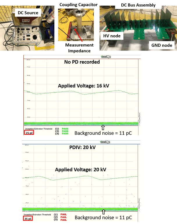
The PCB bus assembly is pictured in Fig. 1. Key E-field control approaches are summarized as follows: 1) All copper conductors are embedded in internal layers to help control peak electric field at the PCB air interface. 2) A multilayer stack-up with internal net-net spacing based on ΔV to the PTH is implemented to provide field grading and help distribute the electric field uniformly across the PCB layer stack. 3) A minimum relative net spacing pattern is used for NPTH and board edge to prevent the surface discharge that will otherwise happen if equal spacing is applied from all the nets to the aperture/edge. 4) An effective shielding technique using a 2D embedded shield layer is applied to reduce surface peak E-field at PCB terminal triple-junction points by moving the peak E-field point along the shielding layer where the E-field limit is higher. The above E-field control methods help achieve PD-free operation greater than the design target of 18 kV. Fig. 2 shows dc PD test results.
