LIBRARY
10 kV, 39 mΩ·cm2 Multi-Channel AlGaN/GaN Schottky Barrier Diodes

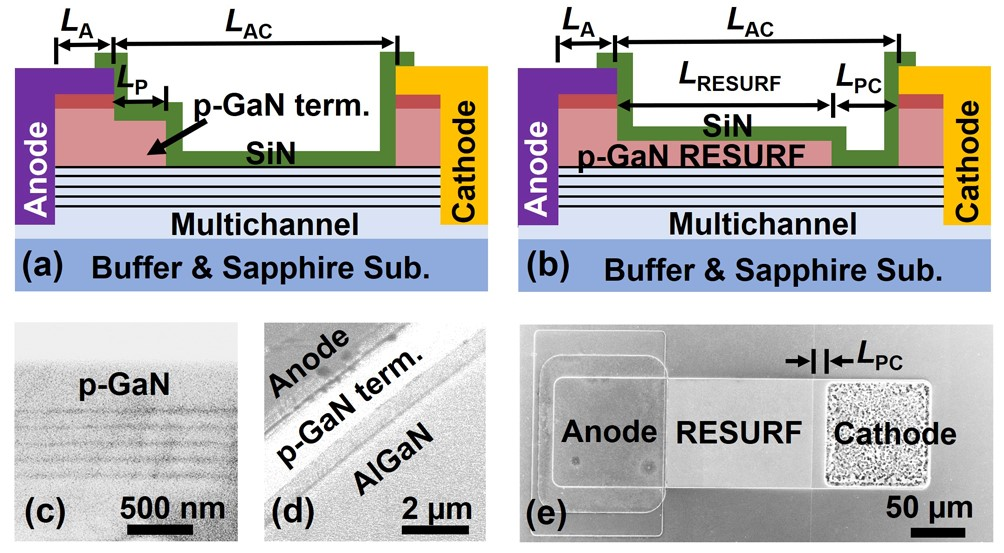
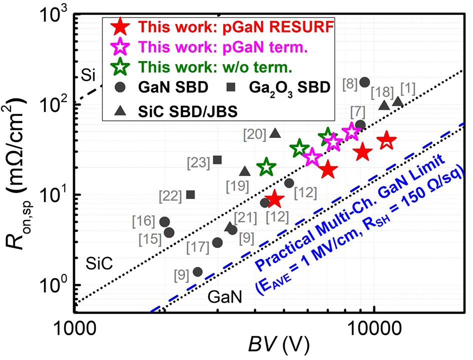
The epitaxial structure consists of a p-GaN cap layer and five AlGaN/GaN channels continuously grown on a low-cost 4-inch sapphire substrate. Fig 1(a) shows a reference sample with the p-GaN termination. A novel device design is proposed for electric field management, i.e., the p-GaN reduced surface field (RESURF) structure, which balances the net charges in the multi-channel at reverse biases (Fig. 1(b)). Fig. 2 benchmarks the RON,SP v.s. BV of our GaN SBDs with the state-of-the-art HV (BV > 2 kV) GaN SBDs, SiC JBS/SBDs, and Ga2O3 SBDs. The SBD with a 98-µm anode-to-cathode length (LAC) shows a BV of 9.15 kV and a specific on resistance (RON) of 29.5 mΩ·cm2, rendering a Baliga's figure of merit (FOM) of 2.84 GW/cm2. The SBD with a 123-µm LAC shows a BV over 10 kV and a RON of 39 mΩ·cm2, which is 2.5-fold lower than the RON of the state-of-the-art 10-kV SiC junction barrier Schottky diodes. The Baliga's FOMs of our 4.6-10 kV GaN SBDs well exceed the SiC unipolar limit. These results show the great promise of GaN for medium- and high-voltage power electronics.


