LIBRARY
Overvoltage Robustness of p-Gate GaN HEMTs in High Frequency Switching up to Megahertz

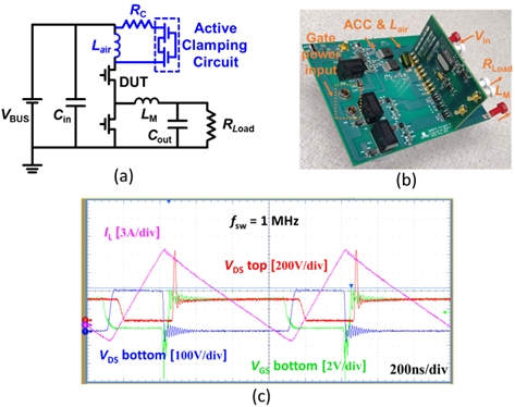
Fig. 1(a) & (b) show the test circuit and the test setup of the high-frequency overvoltage test (HFOT), which consists of a ZVS buck converter and an air core inductor (Lair) to initiate the voltage overshoot at the hard turn-off transient. An ACC, which is connected in parallel with the Lair, turns on after the first VDS overshoot, transferring the surge energy to the ACC loop; the ACC turns OFF before the top switch turns ON, which regulates the overvoltage ringing waveform to contain only one high VDS overshoot pulse. In addition, the energy stored in Lair is fully dissipated in the ON-state power metal-oxide-semiconductor field-effect transistors (MOSFETs) and Rc in each cycle, allowing for the realization of a stable peak VDS. Fig. 1(c) illustrates the sample testing waveforms at 1 MHz.
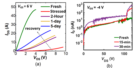
Four devices under test (DUTs) are used in this work: IGOT60R070D1 (DUT#1), EPC2045 (DUT#2), GS66508T (DUT#3), and GS61008T (DUT#4). DUT dynamic breakdown voltage (BVDYN) characterization is first carried out under various switching frequencies fsw. It is found that while DUTs #1 and #2 show a nearly fsw independent BVDYN, DUT #3 and #4 show a considerably reduced BVDYN-SW at high fsw (>200 kHz). Two distinct root causes of the fsw dependent BVDYN are identified through the HFOT stressing at 70% of the BVDYN. DUT #3 shows a drastic (over 30 times), nearly unrecoverable increase in RON after 15 minutes of stressing (Fig. 2(a)); this degradation is a result of severe electron trapping induced in the transient overvoltage.

Meanwhile, DUT #4 shows degradations in the OFF-state leakage current and breakdown voltage (Fig. 2(b)). The humps in the leakage current curve can be explained by the space charge limited current (SCLC).


