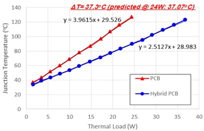
Fig. 1. Device temperature comparison between the PCB and proposed module.
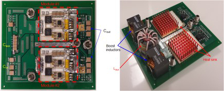
Vehicular power systems are characterized by their stringent requirements for reliability, efficiency, and power density. Along with high-frequency switching to decrease the size of passive components, efficient heat management is a key technique to obtaining high power density, as it can reduce the need for bulky cooling devices such as heat sinks, fans, and liquid coolants. We propose the construction and utilization of a thermally enhanced switching module to lower the system thermal resistance and achieve a compact power system. The proposed thermally enhanced module integrates the semiconductor devices, their drivers and heat sinks by using direct bond copper (DBC): on the top side the DBC is used to assemble the electric components (see Fig. 3(a)), and on the bottom side the heat sink is attached to the DBC (see Fig. 3(b)). The DBC provides a thermal path with low thermal resistance between the thermal source and the thermal sink; i.e., the semiconductor package and air.
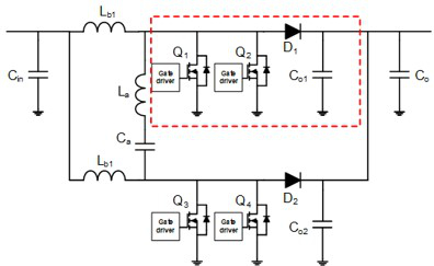
A sample of the proposed module has verified that it suppresses the thermal resistance to 60% of that of its conventional printed circuit board (PCB) counterpart. The slopes of the blue and red curves in Fig. 1 indicate the thermal resistances of the proposed and conventional PCB. The proposed concept is applied to the 2-kW boost converter, of which a circuit diagram is shown in Fig. 2. Components in the dotted box in Fig. 2 are soldered on the DBC of the thermally enhanced module by a vacuum reflow process, as shown in Fig. 3(a), and the module is attached and wired by copper wires and ribbons, as shown in Fig. 3(b).

Fig. 2. 2-kW boost converter configuration. Components in the box are on the DBC of the thermally enhanced module.

Fig. 3. (a) The proposed thermally enhanced switching module.

Fig. 3. (b) Its attachment to PCB.
