LIBRARY
Switching capability evaluation of GaN power FETs using a new intrinsic maxi-mum switching frequency figure-of-merit

A schematic cross-section view of the simulated FET structures are shown in Fig.1. Note that the structure in this figure is not to scale. All the three structures operate in enhancement mode. The MOS channel HEMT and the vertical UMOSFET utilize the MOS channel, while the p-AlGaN gate HEMT adopts the 2DEG channel near the interface of AlGaN/GaN heterojunction.
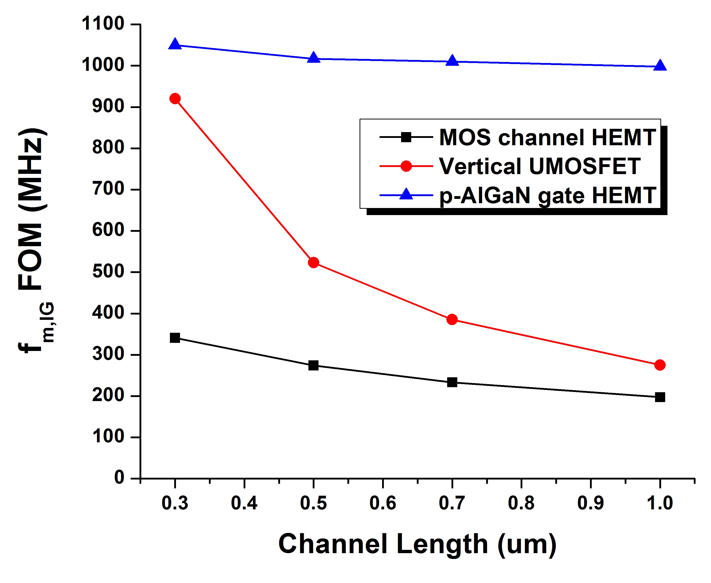
The intrinsic maximum switching frequency fm,IG is defined as a new figure-of-merit; an estimate of the upper limit of the FET switching speed, which allows comparison between the switching capabilities of the different FET designs in the same semiconductor realm as GaN. It is calculated as ID/(2QG), where ID is the on-state drain current, and QG is the gate charge needed to turn on the FET. QG is obtained from the turn-on transient simulation by MEDICI, in which VG shifts from 0 V to VG,on, and VDD is set to 600V for all the structures in order to compare their switching capability at the same voltage rating. The extracted FOM of the lateral MOS channel HEMT, vertical UMOSFET and lateral p-AlGaN gate HEMT are shown in Fig.2. FOM increases when channel length decreases. For the same channel length, FOM of p-AlGaN gate HEMT exceeds that of the other structures with the MOS channel, especially due to its higher 2DEG channel mobility, which gives rise to a larger ID. The FOM of 1.05 GHz is obtained for 0.3 µm channel length. Furthermore, the FOM of the vertical UMOSFET is found to be higher than its MOS channel HEMT counterpart due to its higher ID and smaller QG, which means that the vertical UMOSFET is capable of switching at a higher frequency than the lateral MOS channel HEMT.


