


LIBRARY
High-Density, Fast-Switching 1.2 kV, 90 A Diode-Less SiC MOSFET Half-Bridge Module and Gate Drive Design
Year: 2016
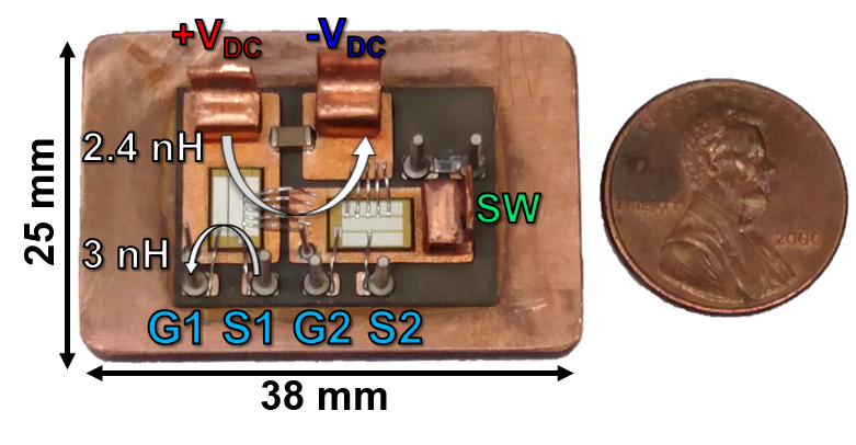
Fig. 1. Fabricated 1.2 kV, 90 A diode-less SiC MOSFET half-bridge module.
The device selected for the power module is the CPM2-1200-0025B 1.2 kV, 25 mω SiC MOSFET from Wolfspeed, a Cree company. Due to the high-current capability of these SiC MOSFETs, only one MOSFET is needed per switch position for this application. The fabricated module is shown in Fig. 1. From the Q3D simulations, it was estimated that the power module has a small power loop inductance of 2.4 nH, and a gate loop inductance of just 3 nH. The module has a power density of 7.8 W/mm3, which is more than two times that of similarly-rated commercial power modules.
In order to realize a 99% efficient inverter, the module must have low switching losses. This can be achieved by switching the MOSFETs quickly; hence a high-speed gate drive with high common-mode immunity must be developed. The initial gate drive specifications are shown in Table I.
Additionally, it is also desirable for the gate drive to have under-voltage lockout (UVLO), overcurrent protection, soft turn-off, and active Miller clamping. The UVLO prevents insufficient voltage from driving the SiC MOSFETs. The overcurrent protection limits the current through the devices. In order to ensure that this current remains within the safe operating range of the device, the overcurrent protection must have a quick response time. When the overcurrent protection is triggered, the driver should turn off the device slowly such that the overvoltage (caused by parasitic inductance in the module and circuitry) is minimized. Finally, active Miller clamping should be employed in order to prevent false turn-on of the MOSFET due to the Miller effect.
The double pulse test was conducted on the bottom and top switches with the designed gate driver. At 600 V and 50 A, with an external resistor of 2.5 ω, a slew rate of 60 V/ns was observed. The half-bridge module was also run in a boost converter, and efficiency as high as 99% was measured. The boost converter waveforms at 450 V output and 15 A inductor current are shown in Fig. 2. Once a proper thermal management system for the module has been devel-oped, the converter will be tested to the full power of 6.74 kW.
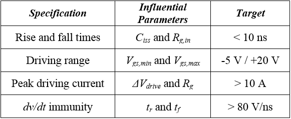
Fig. 2. Initial gate drive specifications
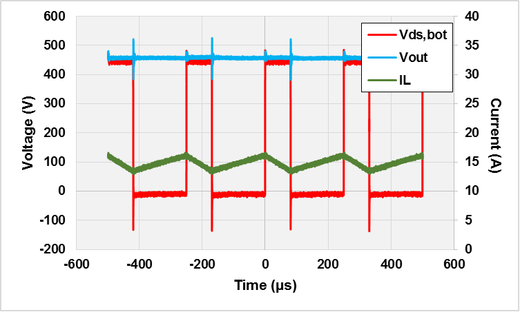
Fig. 3. Experimental waveforms from a boost test with 450 V output, 0.6752 duty cycle, 40 kHz switching with 200 ns dead time.
