


LIBRARY
Insulation design and evaluation via partial discharge (PD) test for power electronics applications
Year: 2017 | Author: Yue Xu | Paper: D4.11
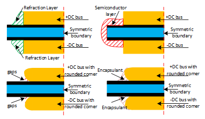
Fig. 1. Practical methods to reduce fringe effect
Insulation evaluations and tests are usually performed for high-voltage line frequency applications, but there has not been much research on insulation evaluation and design for power electronic applications, or under repetitive short rising time impulse excitation. A great deal of work is still worthy of being done for the insulation design and evaluation for the field of power electronics.
Some ways to reduce the fringing effect are summarized and shown in Fig. 1. These methods can help reduce the dielectric stress in the system and thus improve the insulation. The effectiveness of the methods will be proved via Maxwell simulation. The PD measurement setup used in the lab is illustrated in Fig. 2, with a single-void test specimen to verify the effectiveness of the setup. The sensitivity of this setup is around 20 pC and is sufficient to evaluate the insulation for most of the existing parts in power electronics equipment. Finally, a real lab-made laminated bus is depicted in Fig. 3, and its PD behaviour under line frequency excitation is evaluated in Fig. 4. More tests for the PD behaviour under PWM excitation will be done in the future, and ways to improve the insulation for existing parts will be discussed.
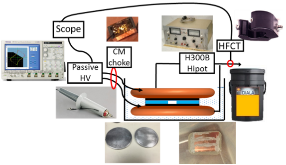
Fig. 2 Block and wire diagram for the PD test setup

Fig. 3 3D drawing of the laminated bus under test
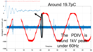
Fig. 4 PD behavior of the laminated bus
